
A surface treatment method of a gallium arsenide substrate

A technology for surface treatment and substrate surface, applied in the field of material processing, can solve the problems of inability to ensure that the substrate surface is completely clean, unfavorable energy saving and emission reduction production efficiency, low processing effect and efficiency, etc., to ensure the quality of interface contact and improve product quality. Yield and device performance, the effect of ensuring surface cleanliness

Inactive Publication Date: 2019-01-04
SHANDONG INSPUR HUAGUANG OPTOELECTRONICS
View PDF8 Cites 2 Cited by
  • Summary
  • Abstract
  • Description
  • Claims
  • Application Information

AI Technical Summary

Problems solved by technology

[0004] At present, the common surface treatment method of gallium arsenide substrate is chemical cleaning or etching to remove pollutants, impurities, organic matter, oxide film, etc. on the surface of the substrate. This method often takes a relatively long time and requires a certain temperature, chemical Reagents, even special equipment and processes, are not conducive to energy saving, emission reduction and production efficiency improvement
[0005] Chinese patent document CN1079579C discloses a semiconductor substrate cleaning method and a semiconductor device manufacturing method. This method mainly immerses the substrate in pure water with a low dissolved oxygen concentration above 60°C. The chemical oxide film on the surface of the substrate cannot guarantee the complete cleanliness of the substrate surface, and the process includes a variety of equipment components, the treatment effect and efficiency are not high, it is a simple surface treatment method
[0006] CN104518056A discloses a method for preparing a reverse polarity red light LED, in which the gallium arsenide substrate corrosion method involved adopts an ammonia solution for corrosion, and the corrosion rate of this method is not easy to control, and the phenomenon of dirty corrosion is easy to occur
[0007] CN105382676A discloses a gallium arsenide wafer polishing method, which is realized by an oxidizing agent, a reducing agent and a mechanical polishing machine. The polishing method is mainly used in materials or devices with high requirements on surface flatness and roughness, and is not suitable for red The polishing of light LED gallium arsenide substrate is also not conducive to improving production efficiency

Method used


Image

  • A surface treatment method of a gallium arsenide substrate

Examples


Embodiment 1

[0023] (1) The gallium arsenide substrate 2 is thinned according to the thickness required by the process, so that the thickness meets the process requirement. Gallium arsenide substrate has no fixed crystal orientation and size requirements;

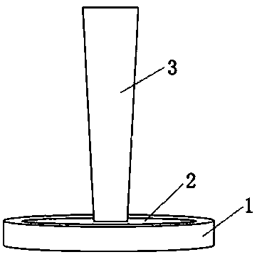
[0024] (2) see figure 1 , place the gallium arsenide substrate 2 to be processed on the stage 1 . The slide table 1 does not interact with the pulsed laser beam 3 and can completely carry the gallium arsenide substrate 2 without a fixed shape requirement.

[0025] (3) Adjust the pulse laser energy density to 0.1J / cm 2 , laser wavelength 248nm, frequency 1Hz;

[0026] (4) Applying the laser adjusted in step (3) to the surface of the gallium arsenide substrate evenly for 10 minutes;

[0027] (5) Turn off the pulsed laser, remove the gallium arsenide substrate obtained in step (4) from the loading stage and place it in deionized water for cleaning for 1 minute;

[0028] (6) drying the gallium arsenide substrate obtained in step (5) wi...

Embodiment 2

[0031] Step (1) and step (2) of this embodiment are the same as embodiment 1.

[0032] (3) Adjust the pulse laser energy density to 4.5J / cm 2 , laser wavelength 532nm, frequency 20Hz;

[0033] (4) Applying the adjusted laser light in step (3) to the surface of the gallium arsenide substrate evenly for 7 minutes;

[0034] (5) Turn off the pulsed laser, remove the gallium arsenide substrate obtained in step (4) from the loading stage and place it in deionized water for cleaning for 5 minutes;

[0035] (6) Drying the gallium arsenide substrate obtained in step (5) with hot nitrogen at a drying temperature of 60° C. for 5 minutes;

[0036] (7) After drying, a gallium arsenide substrate with a clean surface is obtained for subsequent production.

Embodiment 3

[0038] Step (1) and step (2) of this embodiment are the same as embodiment 1.

[0039] (3) Adjust the pulse laser energy density to 10J / cm 2 , laser wavelength 1024nm, frequency 30Hz;

[0040] (4) Applying the adjusted laser light in step (3) to the surface of the gallium arsenide substrate evenly for 4 minutes;

[0041] (5) Turn off the pulsed laser, remove the gallium arsenide substrate obtained in step (4) from the loading stage and place it in deionized water for cleaning for 10 minutes;

[0042] (6) Drying the gallium arsenide substrate obtained in step (5) with hot nitrogen at a drying temperature of 90° C. for 1 minute;

[0043] (7) After drying, a gallium arsenide substrate with a clean surface is obtained for subsequent production.


PUM

PropertyMeasurementUnit
wavelengthaaaaaaaaaa

Abstract

A surface treatment method of a gallium arsenide (GaAs) substrate comprises the following steps: (1) thinning the GaAs substrate; 2) uniformly applying pulsed laser to the surface of the GaAs substrate; (3) cleaning the GaAs substrate after pulsed laser irradiation with deionized water; (4) drying the deionized water washed GaAs substrate with hot nitrogen to obtain a clean GaAs substrate. This method is simple, high proces efficiency, without the introduction of irritant chemicals, with the aid of a pulsed laser, deionized water and hot nitrogen can clean the surface of GaAs substrate, The surface of the treated GaAs substrate is free of organic matter and impurity particles, which ensures the quality of interface contact after subsequent metal evaporation, prevents electrode dropping anddevice voltage abnormality, improves product yield and device performance, ensures surface cleanliness to the maximum extent, and improves production efficiency.

Description

technical field [0001] The invention relates to a surface treatment method of a gallium arsenide substrate used for LED and / or LD, and belongs to the technical field of material processing. Background technique [0002] Gallium arsenide, as an important III-V direct band gap compound semiconductor material, has been widely used in the field of microelectronics and optoelectronic devices due to its high electron mobility, large band gap, and low power consumption. Gallium arsenide is currently the largest, most widely used, and most important compound semiconductor material next to semiconductor silicon. It has shown great development potential in microwave devices and light-emitting devices, especially the current red LED and LD devices. Gallium arsenide is still the mainstream substrate material. [0003] In view of the important application of gallium arsenide substrate in red LED and LD devices, its surface treatment is particularly important, which directly affects the ...

Claims


Application Information

Patent Timeline
Patent Type & Authority Applications(China)
IPC IPC(8): H01L21/02H01L21/8252H01L33/00
CPCH01L21/02008H01L21/02041H01L21/8252H01L33/0062
Inventor 胡夕伦闫宝华刘琦郑兆河肖成峰
Owner SHANDONG INSPUR HUAGUANG OPTOELECTRONICS
Learn More