A trench type insulated gate bipolar transistor and a preparation method thereof

A technology of bipolar transistors and insulated gates, applied in semiconductor/solid-state device manufacturing, semiconductor devices, electrical components, etc., can solve the problem of increasing forward voltage drop, increasing device drift region, forward voltage drop and turn-off loss In order to reduce the conduction voltage drop, optimize the turn-off loss and enhance the conductance modulation effect

Active Publication Date: 2019-01-11
UNIV OF ELECTRONIC SCI & TECH OF CHINA
View PDF3 Cites 14 Cited by
  • Summary
  • Abstract
  • Description
  • Claims
  • Application Information

AI Technical Summary

Problems solved by technology

Therefore, in order to maintain a certain blocking capability of the device in practical applications, technicians have to increase the thickness of the d

Method used


Image

  • A trench type insulated gate bipolar transistor and a preparation method thereof
  • A trench type insulated gate bipolar transistor and a preparation method thereof
  • A trench type insulated gate bipolar transistor and a preparation method thereof

Examples


Embodiment 1

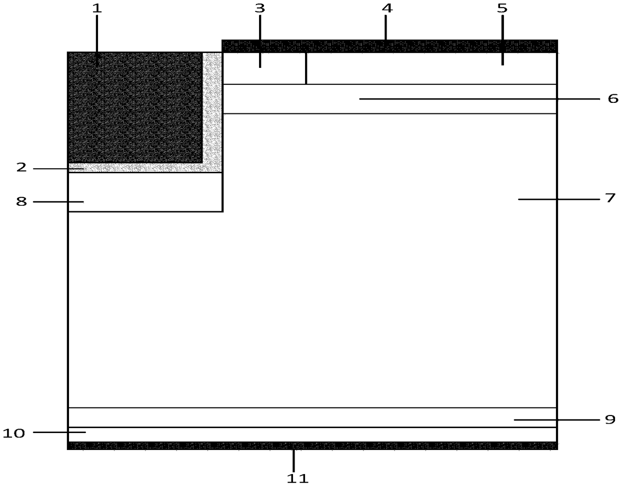
[0053] This embodiment provides a trench-type silicon carbide insulated gate bipolar silicon carbide transistor, the half-cell structure of which is as follows image 3 As shown, it includes: metallized collector electrode 11, P-type silicon carbide collector region 10, N-type silicon carbide field stop layer 9, N-silicon carbide drift region 7, P-type silicon carbide base region 6, N+ silicon carbide emitter region 3. Trench gate structure and emitter metal 4; the metallized collector electrode 11 is located on the back side of the P-type silicon carbide collector region 10, and the N-type silicon carbide field stop layer 9 is located on the front side of the P-type silicon carbide collector region 10. - The silicon carbide drift region 7 is located on the front of the N-type silicon carbide field stop layer 9; the P-type silicon carbide base region 6 and the N+ silicon carbide emitter region 3 are located side by side under the emitter metal 4, wherein the P-type silicon carb...

Embodiment 2

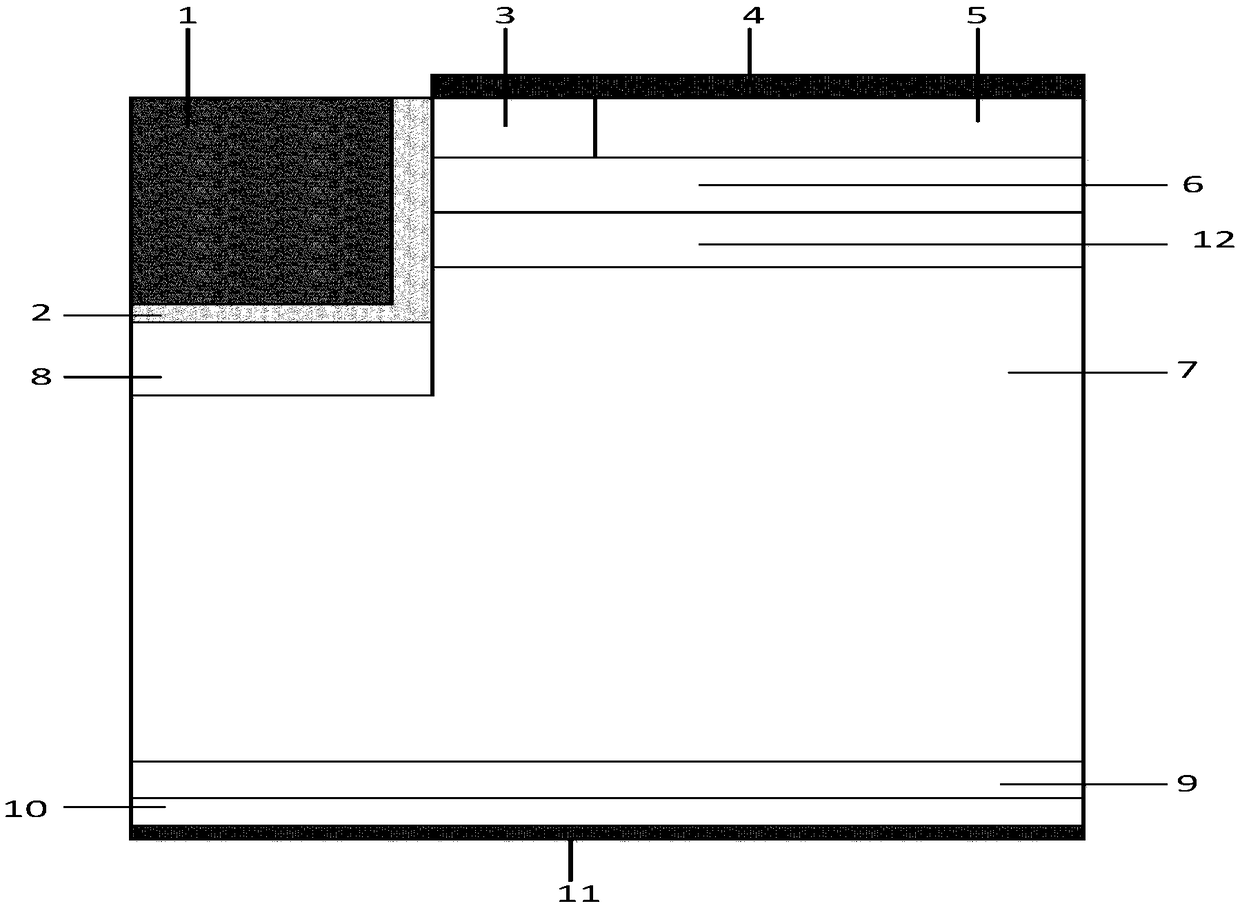
[0059] This embodiment provides a trench-type silicon carbide insulated gate bipolar silicon carbide transistor, the half-cell structure of which is as follows Figure 4 As shown, in this embodiment, on the basis of Embodiment 1, the first P-type silicon layer 13 is set to extend into the lower P-type base region 6 to form a trench, and the first P-type silicon layer 13 is formed in the trench. The bottom and side walls of the groove form a heterojunction with the P-type base region 6 and the N-type emitter region 3; the groove depth of the first P-type silicon layer 13 can be the same as that of the N+ emitter region 3, or it can be different.

[0060] Compared with Embodiment 1, this embodiment reduces the parasitic resistance formed in the P-type base region 6, reduces the voltage drop formed by the hole current in the P-type base region 6, and further suppresses the possible dynamic latch of the device. lock, which improves the high current shutdown capability of the devic...

Embodiment 3

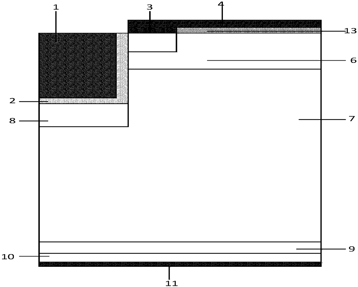
[0062] This embodiment provides a trench-type silicon carbide insulated gate bipolar silicon carbide transistor, the half-cell structure of which is as follows Figure 5 As shown, the schematic cross-sections along the lines AB and CD of the semi-cellular structure are shown in Figure 6 and 7 As shown, this embodiment is based on Embodiment 2, which introduces a second P-type silicon layer 14 in the first P-type shielding layer 8, and the second P-type silicon layer 14 is externally connected to the emitter metal 4. The second P-type silicon layer 14 forms a heterojunction with the first P-type shielding layer 8 .

[0063] Compared with Embodiment 2, this example makes the first P-type shielding layer 8 not in the floating state, thereby solving the problem of the first P-type shielding layer 8 floating in the air. In the off state, although the negative charge in the floating P-type shielding layer can suspend part of the electric field lines, modulate the electric field a...


PUM

PropertyMeasurementUnit
Thicknessaaaaaaaaaa

Abstract

The invention relates to a trench-type insulated gate bipolar transistor and a preparation method thereof, belonging to the technical field of power semiconductors. A semiconductor layer or Schottky contact metal having a relatively small band gap is introduced into the upper surface of the base region of the device adjacent to the outer side of the emitter region, By using heterojunction or Schottky contact as minority carrier barrier to enhance the conductivity modulation effect, the conduction voltage drop is reduced and the tradeoff between forward voltage drop and turn-off loss is optimized. As the heterojunction or Schottky contact introduced by the invention can replace the CS layer functionally, the electric field strength of the PN junction formed in the base region and the driftregion is reduced to improve the breakdown voltage of the device; and the electric field intensity of the gate oxide layer is below the safe value (3MV/cm), so the reliability of the gate oxide layeris ensured. In addition, the fabrication process of the device is simple and controllable, and the device has strong compatibility with the existing process.

Description

technical field [0001] The invention belongs to the technical field of power semiconductors, and in particular relates to a trench type insulated gate bipolar transistor and a preparation method thereof. Background technique [0002] Insulated Gate Bipolar Transistor (IGBT) is a bipolar device controlled by an insulated gate. The higher the non-equilibrium carrier concentration in the body, the more significant the conductance modulation effect and the higher the current density. Figure 1 shows the half-cell structure of a traditional trench IGBT device. When the device is conducting forward conduction, due to the extraction of minority carriers by the reverse-biased PN junction formed by the base region 6 and the drift region 7, its conductance modulation The effect is not significant, resulting in excessive forward voltage drop, and the compromise characteristics are not improved. Such as figure 2 As shown, the conductance modulation effect of the drift region is enhance...

Claims


Application Information

Patent Timeline
IPC IPC(8): H01L29/739H01L29/10H01L29/08H01L29/06H01L21/331
CPCH01L29/0615H01L29/0688H01L29/0817H01L29/1095H01L29/66348H01L29/7397
Inventor 张金平罗君轶赵阳刘竞秀李泽宏张波
Owner UNIV OF ELECTRONIC SCI & TECH OF CHINA
Why Eureka
Try Eureka