Device and method for adsorbing and removing methyl chlorosilane impurities to prepare high-purity trichlorosilane

A technology of high-purity trichlorosilane and monomethyldichlorosilane is applied in chemical instruments and methods, halogenated silanes, silicon compounds, etc., to achieve the effects of prolonging the service cycle, simple process flow, and low equipment investment.

Inactive Publication Date: 2019-01-15
TIANJIN UNIVERSITY OF SCIENCE AND TECHNOLOGY
View PDF5 Cites 15 Cited by
  • Summary
  • Abstract
  • Description
  • Claims
  • Application Information

AI Technical Summary

Problems solved by technology

[0007] The invention provides a device and method for preparing high-purity trichlorosilane by absorbing and removing the impurities of methyl chlorosilane. The trichlorosilane product purified by multi-stage rectification is used as the raw material, a

Method used


Image

  • Device and method for adsorbing and removing methyl chlorosilane impurities to prepare high-purity trichlorosilane

Examples


Embodiment 1

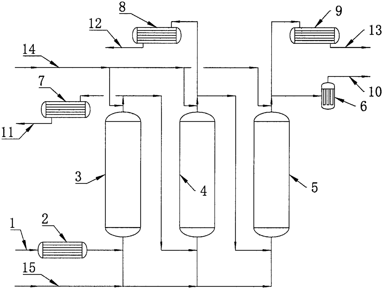
[0035] The trichlorosilane rectification process of an enterprise is as follows: light removal first, then heavy removal, second light removal and second weight removal; the trichlorosilane after the second light removal is taken as the raw material of the adsorption device, and firstly passed through the deep The cooler is cooled to 0°C, then enters the adsorption device at a flow rate of 20ml / min, and passes through the three-stage adsorption columns in sequence (the adsorbent amount of each adsorption column is 200g), the particle size of the semi-carbonized resin adsorbent packed in the A adsorption column 0.6 ~ 0.8mm, the average pore diameter is The specific surface area is 33m2 / g. The dimethyl monochlorosilane directional adsorbent packed in the B adsorption column has a particle size of 800-1600 μm and a pore size of The specific surface area is 700m2 / g. The monomethyldichlorosilane directional adsorbent packed in the C adsorption column has a particle size of 800-...

Embodiment 2

[0041] The trichlorosilane product obtained from the secondary weight removal tower was analyzed, and compared with the trichlorosilane product obtained from the second weight removal tower, a primary rectification purification was added. Among them, the theoretical plate number of the secondary weight removal tower is 240, and the reflux ratio is 6.2. The analysis results are shown in Table 2.

[0042] [Table 2]

[0043]

[0044] The same trichlorosilane material, after primary distillation and purification, the content of dimethyl monochlorosilane can only be reduced from 0.8ppmw to 0.4ppmw, and the content of monomethyldichlorosilane can only be reduced from 1.0ppmw to 0.5 ppmw, and above the lower detection limit of the analytical instrument. For the removal of trace impurities with relatively close boiling points, rectification technology is not as effective as adsorption technology, and cannot meet the production of electronic-grade polysilicon.


PUM

PropertyMeasurementUnit
Particle sizeaaaaaaaaaa
Specific surface areaaaaaaaaaaa
Particle sizeaaaaaaaaaa

Abstract

The invention relates to a device and a method for adsorbing and removing methyl chlorosilane impurities to prepare high-purity trichlorosilane. According to molecule size difference of different methyl chlorosilane monomers, an adsorbent with an oriented adsorption function is prepared; three adsorption columns are respectively filled with a pretreatment adsorbent and the oriented adsorbent; trichlorosilane which is rectified and purified in a multilevel mode is utilized as a raw material, a designed multilevel adsorption device is utilized to perform oriented adsorption, the content of carbon impurities in the adsorbed trichlorosilane is greatly reduced, and electronic-grade polycrystalline silicon production can be realized. Meanwhile, as the adsorption columns are filled with the adsorbent which can perform oriented adsorption on the trichlorosilane, dimethyl chlorosilane and methyl dichlorosilane can be selectively adsorbed in an adsorption process; thus, the dimethyl chlorosilaneand the methyl dichlorosilane can be effectively separated, the dimethyl chlorosilane and the methyl dichlorosilane can be respectively utilized as organosilicone products to be directly recycled after being desorbed, aftertreatment technologies are reduced, energy consumption is saved, and economic benefits are improved.

Description

technical field [0001] The invention belongs to the technical field of high-purity trichlorosilane preparation, and relates to a process for adsorbing and removing methylchlorosilane impurities, in particular to an adsorption device and method for methylchlorosilane compounds in trichlorosilane. Among them, trichlorosilane is derived from the material after the existing multi-stage rectification and impurity removal device. Background technique [0002] Polycrystalline silicon is used as the raw material for manufacturing semiconductor devices. Carbon impurities in silicon crystals will accelerate the formation of oxygen precipitation, thereby inducing secondary defects such as crystal dislocation and stacking faults in the manufacturing process of semiconductor devices. Once the carbon content in polysilicon is too high, it cannot be removed again in subsequent processing, thus seriously affecting the electrical performance of semiconductor devices. Therefore, for semicond...

Claims


Application Information

Patent Timeline
IPC IPC(8): C01B33/107
CPCC01B33/1071C01B33/10784
Inventor 王红星陈锦溢华超刘洋
Owner TIANJIN UNIVERSITY OF SCIENCE AND TECHNOLOGY
Why Eureka
Try Eureka