A high early voltage bipolar device and its manufacturing method

A technology of bipolar devices and manufacturing methods, which is applied in semiconductor/solid-state device manufacturing, electrical components, semiconductor devices, etc., and can solve the problems of increased output fluctuations of reference sources, low threshold voltage of parasitic PMOS, and low impurity concentration on the surface of epitaxial layers, etc. , to achieve the effect of increasing the Early voltage, increasing the threshold voltage, and reducing the Early effect

Active Publication Date: 2021-12-14
XIAN MICROELECTRONICS TECH INST
View PDF0 Cites 0 Cited by
  • Summary
  • Abstract
  • Description
  • Claims
  • Application Information

AI Technical Summary

Problems solved by technology

[0003] Traditional NPN transistors have low Early voltage and significant Early effect, which affect the accuracy of the circuit in integrated circuits with high demand. For example, when used as a reference source, the output fluctuation of the reference source increases due to the influence of the Early effect.
For NPN transistor circuits with high operating voltage, due to the low impurity concentration on the surface of the epitaxial layer, the parasitic PMOS threshold voltage is low, which affects the metal wiring of the circuit and the lower limit of the operating voltage

Method used


Image

  • A high early voltage bipolar device and its manufacturing method
  • A high early voltage bipolar device and its manufacturing method
  • A high early voltage bipolar device and its manufacturing method

Examples


Embodiment 1

[0069] Adopt novel vertical NPN transistor of the present invention, apply OP77 bipolar integrated circuit, the double-layer epitaxy result that adopts is as follows:

[0070] 1) The process design of the first epitaxial layer is: the thickness is 15 μm, and the resistivity is 6.0Ω·cm;

[0071] 2) The process design of the second epitaxial layer is as follows: the thickness is 2 μm, and the resistivity is 3.2 Ω·cm.

[0072] The effect of using this structure:

[0073] The voltage gain of the product is increased from 130db to 135db, which meets the requirements of use.

Embodiment 2

[0075] For 50V high-precision high-voltage bipolar integrated circuits, the traditional epitaxial process conditions are: thickness 13 μm, resistivity 4Ω cm; using double-layer epitaxial process, the first layer epitaxial process design is: thickness 15 μm, 6Ω cm; second layer The epitaxial process design is: thickness 2μm, resistivity 3.2Ω cm;

[0076] The layout structure of the NPN tube is: the base area is 26 μm × 26 μm, and the emission area is 10 μm × 10 μm.

[0077] The dielectric structure under the parasitic PMOS metal is: 600nm SiO 2 and 100nm Si 3 N 4 .

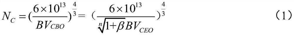
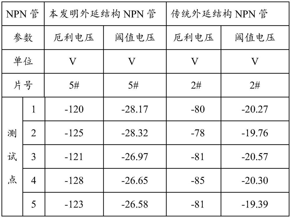
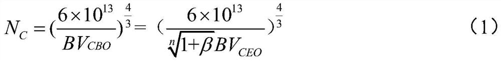
[0078] Early voltage test conditions: Ic 0.5mA, see Table 1 for comparative test results.


PUM

PropertyMeasurementUnit
thicknessaaaaaaaaaa
thicknessaaaaaaaaaa
electrical resistivityaaaaaaaaaa

Abstract

The invention discloses a high Early voltage bipolar device and a manufacturing method thereof. The bipolar device includes three metal wirings and a substrate; an N buried layer, a first epitaxial layer, a second epitaxial layer and SiO 2 layer; 3 metal wires pass through the SiO 2 After the lead-out hole set on the layer, respectively connect the lead-out region of the collector region, the emitter region and the P-type base region; the lead-out region of the collector region and the P-type base region are located inside the second epitaxial layer, and the emitter region is located in the P-type base region Inside; P-type isolation regions are set on both sides of the bipolar device. The main improvement of the method is that it includes performing the first epitaxial process on the substrate to form the first epitaxial layer; performing the second epitaxial process on the first epitaxial layer to form the second epitaxial layer; through the design of the double epitaxial layer, it can Effectively increase the Early voltage, reduce the Early effect, and improve the precision of the integrated circuit; at the same time, the threshold voltage of the parasitic PMOS tube is increased, the metal wiring of the circuit is more convenient, and the working voltage range is expanded.

Description

technical field [0001] The invention belongs to the field of performance improvement of semiconductor devices, and relates to a high Early voltage bipolar device and a manufacturing method thereof. Background technique [0002] NPN transistor is a transistor structure often used in bipolar integrated circuits. In the production of traditional bipolar integrated circuits, an N-type epitaxial layer with desired resistivity and thickness is deposited on a P-type substrate, and is formed by ion implantation or diffusion process. The P-type impurity-doped base region, on the base region and the epitaxial layer, ion implantation or diffusion process is used to form the N-type impurity-doped emitter region and the lead-out region of the collector region, that is, the N-type epitaxial layer is selectively The P-type impurity doping forms the base region, and then selectively N-type impurity doping is performed on the P-type base region to form the emitter region, and at the same tim...

Claims


Application Information

Patent Timeline
Patent Type & Authority Patents(China)
IPC IPC(8): H01L29/732H01L29/06H01L29/78H01L21/331H01L21/336
CPCH01L29/0603H01L29/66272H01L29/66666H01L29/732H01L29/7827
Inventor 任永宁陈宝忠孙有民王清波刘如征葛洪磊马朝柱刘依思
Owner XIAN MICROELECTRONICS TECH INST
Why Eureka
Try Eureka