A kind of translucent perovskite solar cell and its preparation method
A solar cell and perovskite technology, which is applied in semiconductor/solid-state device manufacturing, circuits, electrical components, etc., can solve the problems that hinder the development and utilization of translucent perovskite solar cells, and achieve transparency easily, high processing efficiency, and reduce Active area effect
- Summary
- Abstract
- Description
- Claims
- Application Information
AI Technical Summary
Problems solved by technology
Method used
Image
Examples
Embodiment 1
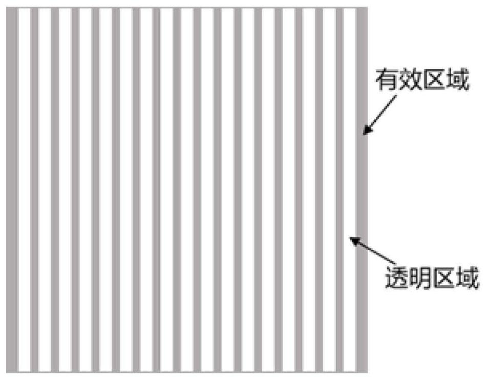
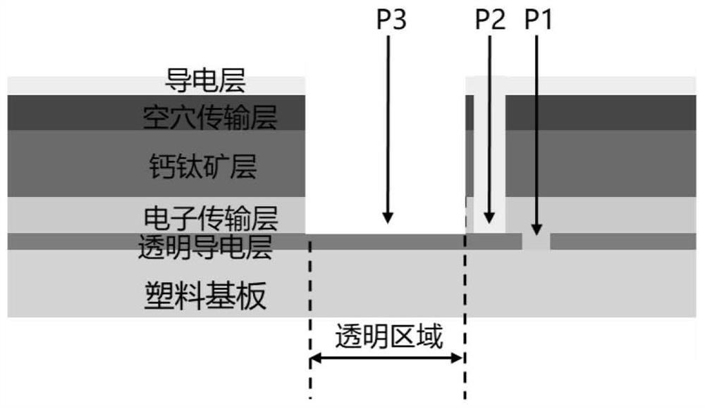
[0026] like figure 1 As shown, a preparation method of a translucent perovskite solar cell includes the following steps:
[0027] (1) Use an ultrafast laser to scribe a 5cm*5cm glass substrate containing an ITO transparent conductive layer, and cut the transparent conductive layer (P1). The tangent spacing is 0.5mm, and the width of a single small battery is 0.5mm. The tangential processing parameters are: picosecond mode, the repetition frequency is 200k Hz, the laser power is 15W, the scanning speed of the galvanometer is 1000mm / s, and the width of the etching line is 30μm; after the cutting is completed, the substrate is cleaned;
[0028] (2) Scratch a layer of tin oxide electron transport layer by Slot-die on the cleaned substrate;
[0029] (3) spin-coating perovskite and spiro-OMeTAD hole transport layers on the tin oxide electron transport layer;
[0030] (4) The functional layers (electron transport layer, perovskite light absorption layer and hole transport layer) ar...
Embodiment 2
[0036] like figure 1 As shown, a preparation method of a translucent perovskite solar cell includes the following steps:
[0037] (1) Use an ultrafast laser to scribe a 10cm*10cm glass substrate containing an FTO transparent conductive layer, and cut the transparent conductive layer (P1). The tangential processing parameters are: picosecond mode, the repetition frequency is 500k Hz, the laser power is 14W, the scanning speed of the galvanometer is 900mm / s, and the width of the etching line is 30μm; after the cutting is completed, the substrate is cleaned;
[0038] (2) prepare a layer of tin oxide electron transport layer by chemical bath deposition on the cleaned substrate;
[0039] (3) spin-coating the perovskite light absorption layer and the spiro-OMeTAD hole transport layer on the tin oxide electron transport layer;
[0040] (4) The functional layers (electron transport layer, perovskite light absorption layer and hole transport layer) are cut by ultrafast laser, but the...
PUM
| Property | Measurement | Unit |
|---|---|---|
| thickness | aaaaa | aaaaa |
| transmittivity | aaaaa | aaaaa |
| energy conversion efficiency | aaaaa | aaaaa |
Abstract
Description
Claims
Application Information


