CMOS SPAD (Single Photon Avalanche Diode) photoelectric device with deep N well adopting inverse doping distribution

A photoelectric device, reverse doping technology, applied in the direction of electrical components, semiconductor devices, circuits, etc., can solve the problem of band tunneling effect, increase the dark current value of the device, and is not conducive to improving the noise performance of the device, etc.

Inactive Publication Date: 2019-01-29
重庆亚川电器有限公司
View PDF3 Cites 1 Cited by
  • Summary
  • Abstract
  • Description
  • Claims
  • Application Information

AI Technical Summary

Problems solved by technology

[0004] (However, the use of this technology makes the photogenerated carriers prone to band tunneling effect in the event of avalanche breakdow

Method used


Image

  • CMOS SPAD (Single Photon Avalanche Diode) photoelectric device with deep N well adopting inverse doping distribution
  • CMOS SPAD (Single Photon Avalanche Diode) photoelectric device with deep N well adopting inverse doping distribution
  • CMOS SPAD (Single Photon Avalanche Diode) photoelectric device with deep N well adopting inverse doping distribution

Examples


Embodiment Construction

[0020] The technical solutions in the embodiments of the present invention will be described clearly and in detail below with reference to the drawings in the embodiments of the present invention. The described embodiments are only some of the embodiments of the invention.

[0021] The technical scheme that the present invention solves the problems of the technologies described above is:

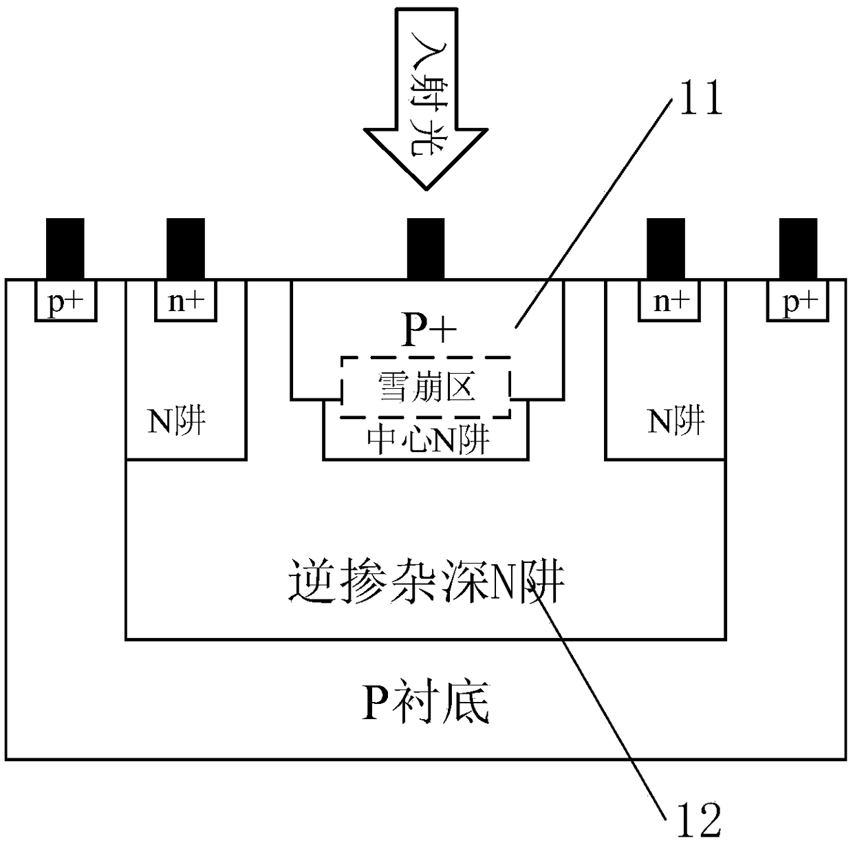
[0022] Such as figure 1 Shown is the structure diagram of the new CMOS SPAD optoelectronic device. It can be seen from the figure that the device is a planar structure composed of P+ / central N well / counter-doped deep N well / P substrate. Among them, the P+ / central N well constitutes the avalanche region of the device (corresponding to region 11 in the figure), and the photogenerated carriers undergo impact ionization in this region and multiply to form a current that can be observed by the naked eye to realize photoelectric conversion. The reverse doping deep N well constitutes the photon ...


PUM

PropertyMeasurementUnit
Thicknessaaaaaaaaaa

Abstract

The invention relates to a CMOS SPAD (Single Photon Avalanche Diode) photoelectric device with a deep N well adopting inverse doping distribution, which comprises a P substrate, wherein the P substrate is provided with a deep N well, a central N well and a P+ layer, two sides of the deep N well are provided with N wells, the deep N well adopts an inverse doping distribution structure, that is, thedeep N well close to the device surface is low in concentration and the concentration of the deep N well increases along the increase in vertical depth away from the device surface, the transverse diffusion exists between the two lateral N wells and the central N well in the deep N well, an n- virtual protection ring is formed at the edge of a PN junction, incident photons are mainly absorbed bythe deep N well when shooting to the internal part of the device, most of the photons can be utilized by the P+ layer/central N well junction to form photon-generated carriers, and only a few of the photons penetrate through the deep N well and form photon-generated carriers on the P substrate. The photon detection efficiency of the device is improved by mainly increasing the thickness of an absorption region of the device and optimizing the quantum efficiency of the device.

Description

technical field [0001] The invention belongs to the field of semiconductor photoelectric detection and sensing, and relates to the structural design of an APD photoelectric device, in particular to the design of a CMOS SPAD photoelectric device with high photon detection efficiency. Background technique [0002] Single photon avalanche diode (Single Photo Avalanche Diode) is widely used in automotive electronics, three-dimensional imaging, instrumentation, biophotonics, fluorescence lifetime imaging and other fields due to its single photon sensitivity. A semiconductor photodetector with a PN junction structure in leather mode (reverse bias voltage greater than breakdown voltage). When photons irradiate the PN junction, the photo-generated carriers are accelerated to the avalanche region and produce a multiplication effect, so that single photons can trigger a large current pulse signal. With the expansion of application fields, the performance requirements for SPADs are ge...

Claims


Application Information

Patent Timeline
IPC IPC(8): H01L31/0352H01L31/107
Inventor 刘淑芸王巍张瑜
Owner 重庆亚川电器有限公司
Why Eureka
Try Eureka