Flexible transient silicon thin film photodetector with MSM structure

A technology of photodetectors and silicon thin films, applied in circuits, electrical components, semiconductor devices, etc., can solve the problems of restricting the practical application of devices, failure to respond, slow degradation rate and limiting the transient performance of silicon devices, etc., so as to improve the photoelectric detection capability , avoid damage, and expand the effect of ultraviolet light detection ability

Active Publication Date: 2019-02-01
XIDIAN UNIV
View PDF5 Cites 4 Cited by
  • Summary
  • Abstract
  • Description
  • Claims
  • Application Information

AI Technical Summary

Problems solved by technology

However, ultra-thin silicon materials cannot respond to ultraviolet light with shorter wavelengths, which restricts the practical application of devices
At the same time, silicon semiconductor materials limit the transient performance of silicon devices due to their slow degradation rates.

Method used


Image

  • Flexible transient silicon thin film photodetector with MSM structure
  • Flexible transient silicon thin film photodetector with MSM structure

Examples


Embodiment 1

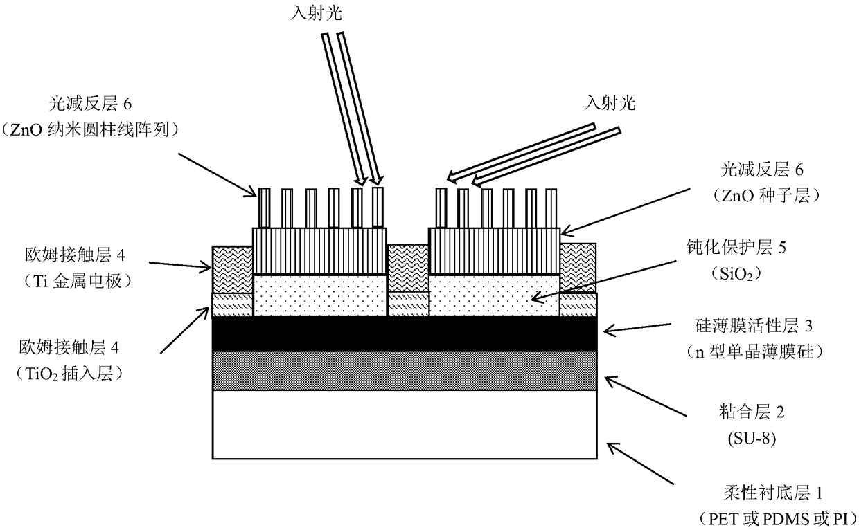
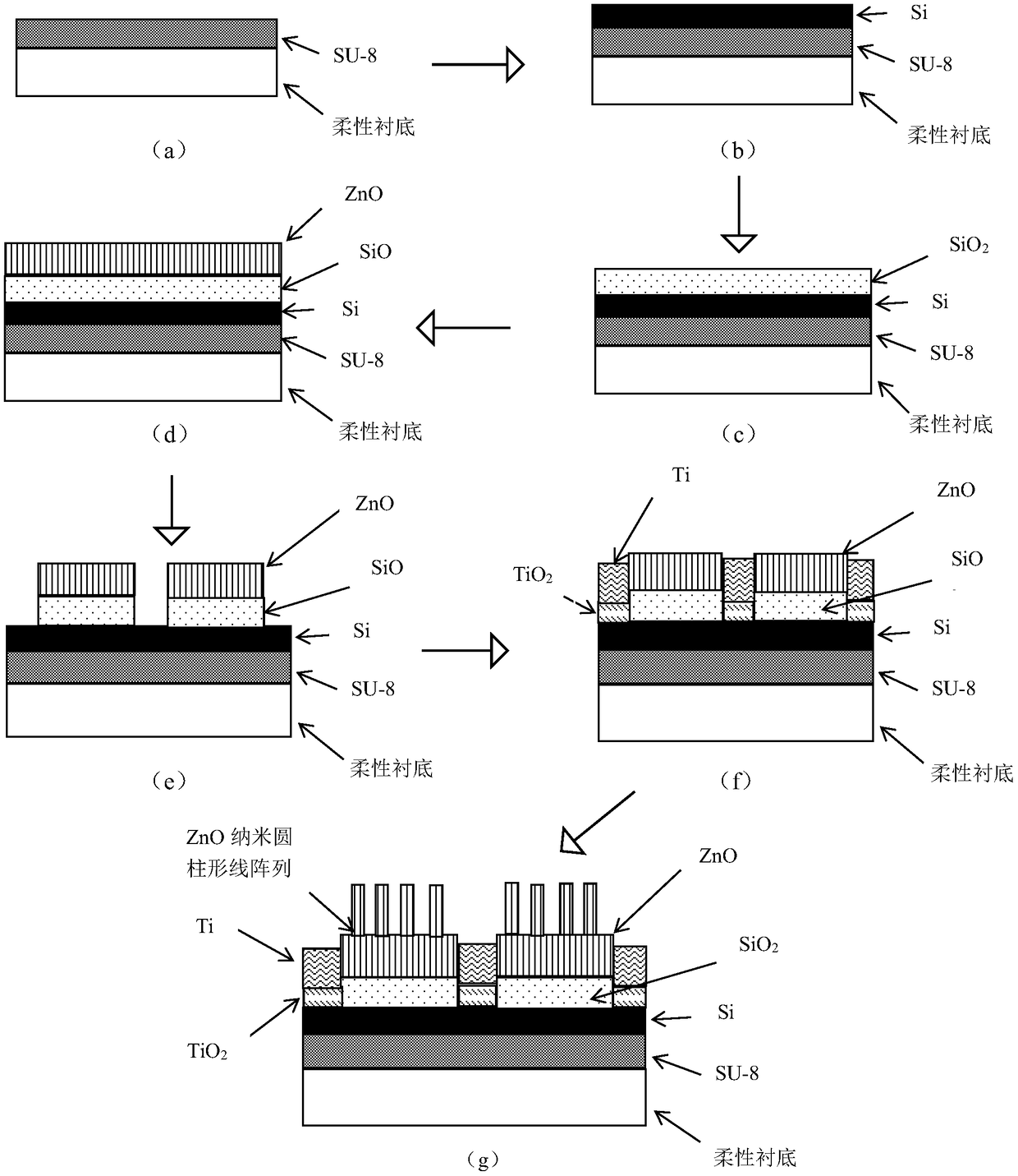
[0038] Example 1, preparing a polyethylene terephthalate PET substrate photodetector grown by magnetron sputtering with a ZnO seed layer thickness of 100 nm.

[0039] Step 1, cleaning the silicon SOI substrate and the polyethylene terephthalate PET flexible substrate on the insulating substrate.

[0040] 1.1) The silicon SOI substrate on the insulating substrate with a thickness of 180nm and the flexible polyethylene terephthalate PET substrate with a thickness of 0.9mm were placed in 10% Decon90 deionized aqueous solution and ultrasonically cleaned for 15min , then placed in deionized water for ultrasonic cleaning for 5 minutes, then placed in acetone for ultrasonic cleaning for 20 minutes, and then placed in absolute ethanol for ultrasonic cleaning for 20 minutes;

[0041] 1.2) Blow dry with nitrogen gun after cleaning, and then in O 2 Hydrophilic treatment for 10 minutes under the environment.

[0042] Step 2, preparing etching holes on the SOI substrate.

[0043] 2.1) P...

Embodiment 2

[0068] Example 2, preparing a polyimide PI substrate photodetector grown by an aqueous solution spin coating method with a ZnO seed layer thickness of 150 nm.

[0069] Step 1, cleaning the silicon SOI substrate and polyimide PI flexible substrate on the insulating substrate.

[0070] The silicon SOI substrate on the insulating substrate with a thickness of 200 nm and the polydimethylsiloxane PDMS flexible substrate with a thickness of 1.2 mm were cleaned, and the cleaning process was the same as step 1 in Embodiment 1.

[0071] Step 2, preparing etching holes on the SOI substrate.

[0072] Carry out photolithography on the SOI substrate after cleaning, it is identical with 2.1) of the step 2 of embodiment 1;

[0073] The conditions of the etching step are the same as 2.2) of Step 2 in Example 1 except that the etching time is 70 s.

[0074] Step 3, transferring the silicon thin film active layer.

[0075] Spin-coat SU-8 photoresist with a thickness of 500nm on the cleaned p...

Embodiment 3

[0094] Example 3, preparing a polydimethylsiloxane PDMS substrate photodetector grown by an organic solvent spin coating method with a ZnO seed layer thickness of 200 nm.

[0095] Step A, cleaning the silicon SOI substrate and the polydimethylsiloxane PDMS flexible substrate on the insulating substrate.

[0096] The silicon SOI substrate on the insulating substrate with a thickness of 220 nm and the polydimethylsiloxane PDMS flexible substrate with a thickness of 1.5 mm were cleaned, and the cleaning process was the same as step 1 in Embodiment 1.

[0097] Step B, preparing etching holes on the SOI substrate.

[0098] Carry out photolithography on the SOI substrate after cleaning, it is identical with 2.1) of the step 2 of embodiment 1;

[0099] The conditions of the etching step are the same as 2.2) of Step 2 in Example 1 except that the etching time is 80 s.

[0100] Step C, transferring the silicon thin film active layer.

[0101] The step of transferring the silicon thi...


PUM


Abstract

The invention discloses a flexible transient silicon thin film photodetector with an MSM structure, which mainly solves the problem that the existing photodetector can not simultaneously satisfy the flexible and transient degradable characteristics. The flexible transient silicon thin film photodetector with an MSM structure comprises a flexible substrate layer (1), a bonding layer (2), a siliconthin film active layer (3), an ohmic contact layer (4), a passivation protection layer (5), and a light reflection reduction layer (6), wherein the silicon thin film active layer adopts n-type singlecrystal light doped thin film silicon; a TiO2 insertion layer is arranged in the ohmic contact layer to improve ohmic contact and avoid damages of a high temperature process to the flexible substrate;and the light reflection reduction layer adopts a ZnO seed layer-ZnO nano-cylindrical line array composite structure, high reflection reduction and light trapping can be realized, the absorption angle of the device is widened, the ultraviolet light detection ability is expanded, and the transient degradability is realized. the flexible and transient characteristics of the photodetector an be realized at the same time, and the photodetector can be applied to ultraviolet astronomy, medicine, biology, sky communication, flame detection and pollution monitoring.

Description

technical field [0001] The invention belongs to the field of semiconductor optoelectronic devices, in particular to a flexible transient silicon thin film photodetector with an MSM structure. Can be used in ultraviolet astronomy, medicine, biology, sky communication, flame detection and pollution monitoring. technical background [0002] In today's society, flexible electronics are changing the way we make and use electronic devices. Many existing applications, such as human implantable electronics, bendable tissues, etc., are driving the development of flexible electronics. This in turn creates a solid foundation for many future applications such as mHealth, wearable systems, smart cities and the Internet of Things. For example, relevant institutions and enterprises in various countries around the world have also increased their research and development efforts. In the past few years, flexible electronics have achieved significant development from nanostructures, printed ...

Claims


Application Information

Patent Timeline
Patent Type & Authority Applications(China)
IPC IPC(8): H01L31/0216H01L31/0224H01L31/108H01L31/18
CPCH01L31/02161H01L31/022408H01L31/1085H01L31/1804H01L31/1868Y02P70/50
Inventor 张春福陈大正杜丰羽张家祺常晶晶林珍华习鹤张进成郝跃
Owner XIDIAN UNIV
Why Eureka
Try Eureka