Supercharge Your Innovation With Domain-Expert AI Agents!

Photoelectric detection diode based on diamond/InP/SiC double heterojunction and preparation method of diode

A photoelectric detection and double heterojunction technology, which is applied in the field of microelectronics, can solve the problems of weak light absorption ability and weak ultraviolet detection ability, so as to improve light absorption ability, reduce low leakage current, and improve device reliability. Effect

Active Publication Date: 2019-02-12
XIDIAN UNIV
View PDF3 Cites 0 Cited by
  • Summary
  • Abstract
  • Description
  • Claims
  • Application Information

AI Technical Summary

Problems solved by technology

[0003] A photodetector diode is a semiconductor device based on a PN junction. It can generally measure ultraviolet light to infrared light. Existing photodetector diodes are generally photodetector diodes based on SiC, GaN, ZnO and other materials, which belong to far-ultraviolet detection diodes. Its detection wavelength is generally less than 220nm, and there are still many problems in the current photodetection diodes, such as weak light absorption ability and weak ultraviolet detection ability, etc.

Method used


Image

  • Photoelectric detection diode based on diamond/InP/SiC double heterojunction and preparation method of diode
  • Photoelectric detection diode based on diamond/InP/SiC double heterojunction and preparation method of diode
  • Photoelectric detection diode based on diamond/InP/SiC double heterojunction and preparation method of diode

Examples


Embodiment 1

[0042] Please also see figure 1 , Figure 2a to Figure 2g , image 3 as well as Figure 4 , figure 1 It is a flow chart of a method for preparing a photodetection diode based on a diamond / InP / SiC double heterojunction provided by an embodiment of the present invention; Figure 2a-Figure 2g A schematic diagram of the preparation process of a photodetector diode based on a diamond / InP / SiC double heterojunction provided by an embodiment of the present invention; image 3 A schematic structural diagram of a first mask plate provided by an embodiment of the present invention; Figure 4 A schematic structural diagram of a second mask plate provided by an embodiment of the present invention. The preparation method of the present embodiment comprises the following steps:

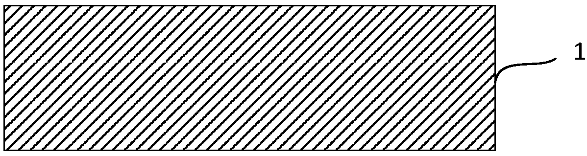
[0043] S1: Continuously grow a homoepitaxial layer, an InP layer and a diamond layer on the upper surface of the SiC substrate;

[0044] Specifically, the S1 includes:

[0045] S11: Using a PECVD (Plasma Enh...

Embodiment 2

[0076] See Figure 5 and Figure 6 , Figure 5 A schematic cross-sectional view of a photodetector diode based on a diamond / InP / SiC double heterojunction provided for an embodiment of the present invention; Figure 6 A schematic top view of a photodetector diode based on a diamond / InP / SiC double heterojunction provided by an embodiment of the present invention. The photodetection diode based on the diamond / InP / SiC double heterojunction of this embodiment includes bottom electrode 5, substrate 1, N-type homoepitaxial layer 2, InP layer 3, N-type diamond layer 4, Light absorbing layer 7 and top electrode 6, wherein, N-type homoepitaxial layer 2 is made of SiC material doped with N element; InP layer 3 is made of P-type InP material doped with N element, N-type diamond layer 4 Made of diamond material doped with N, P, O or S elements.

[0077] Further, in this embodiment, the substrate 1 is made of N-type 4H-SiC or 6H-SiC material, and the N-type homoepitaxial layer 2 is dope...


PUM

PropertyMeasurementUnit
thicknessaaaaaaaaaa
thicknessaaaaaaaaaa
thicknessaaaaaaaaaa

Abstract

The invention relates to a photoelectric detection diode based on diamond / InP / SiC double heterojunction and a preparation method of the diode. The method includes the steps: continuously growing a homogeneous epitaxial layer, an InP layer and a diamond layer on the upper surface of an SiC substrate; growing a first metal material on the upper surface of the diamond layer to form a light absorptionlayer; growing a second metal layer on the lower surface of the SiC substrate to form a bottom electrode; growing a third metal material on the upper surface of the light absorption layer to form a top electrode to prepare the photoelectric detection diode based on the diamond / InP / SiC double heterojunction. According to the photoelectric detection diode based on the diamond / InP / SiC double heterojunction and the preparation method of the diode, a diamond material is applied to the light absorption layer, the light transmission rate of the material in a solar blind area is high, the light absorption capability of the light absorption layer is improved, and the device performance of the photoelectric detection diode can be greatly improved.

Description

technical field [0001] The invention belongs to the technical field of microelectronics, and in particular relates to a diamond / InP / SiC double heterojunction-based photodetection diode and a preparation method thereof. Background technique [0002] With the continuous deepening of research and exploration in medical temperature measurement, aerospace, radar detection and other fields in recent years, production and development have higher and higher requirements for light, especially ultraviolet light and other related detectors, such as photoelectric countermeasures, mid-ultraviolet countermeasures and opposition Resistance is increasingly favored by the military. The wave band with a wavelength of 10-400nm in electromagnetic waves is called ultraviolet radiation, which is different from both infrared radiation and visible light radiation; among them, the spectral region in which the ultraviolet rays from solar radiation are almost completely absorbed by the atmosphere is c...

Claims


Application Information

Patent Timeline
Patent Type & Authority Applications(China)
IPC IPC(8): H01L31/18H01L31/028H01L31/0304H01L31/11
CPCH01L31/028H01L31/0304H01L31/11H01L31/1804H01L31/1852Y02E10/544Y02E10/547Y02P70/50
Inventor 王悦湖张菊王雨田张玉明宋庆文汤晓燕张艺蒙
Owner XIDIAN UNIV
Features
  • R&D
  • Intellectual Property
  • Life Sciences
  • Materials
  • Tech Scout
  • Unparalleled Data Quality
  • Higher Quality Content
  • 60% Fewer Hallucinations
Learn More