Metal nano-cluster doped memristor and method for preparing same

A metal nanocluster and memristor technology, applied in the field of microelectronics, can solve the problems of poor retention characteristics, slow erasing and writing speed, and poor cycle tolerance, and achieve fast erasing and writing speed, low switching voltage, and good memristive switching effect of effect

Active Publication Date: 2019-02-12
XIAMEN UNIV
View PDF6 Cites 9 Cited by
  • Summary
  • Abstract
  • Description
  • Claims
  • Application Information

AI Technical Summary

Problems solved by technology

However, practical memristor products have not been launched for a long time, because the excellent properties reported so far are realized in different memristors, and th...

Method used


Image

  • Metal nano-cluster doped memristor and method for preparing same
  • Metal nano-cluster doped memristor and method for preparing same
  • Metal nano-cluster doped memristor and method for preparing same

Examples


preparation example Construction

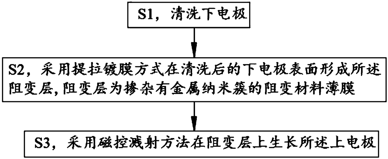
[0033] The present invention also proposes a method for preparing the above-mentioned memristor doped with metal nanoclusters, which includes:

[0034] S1, cleaning the lower electrode;

[0035] S2, forming the resistive layer on the surface of the lower electrode after cleaning by using a pull-coating method;

[0036] S3, growing the upper electrode on the resistive layer by using a magnetron sputtering method.

[0037] In step S1, using the ITO conductive glass to clean refers to decontaminating the ITO conductive glass, for example, immersing it in an organic solution such as acetone for ultrasonic cleaning.

[0038] In step S2, the step of forming the resistive layer on the surface of the lower electrode after cleaning by means of pulling coating includes:

[0039] S21, preparing a natural protein solution. Specific steps include:

[0040] (1) Put the natural silkworm cocoons in a weak alkali solution (such as 3-5 g / L sodium bicarbonate solution), heat and boil for 2...

Embodiment 1

[0054] This embodiment provides a gold nanocluster doped memristor, which is prepared according to the following steps:

[0055] (1) Cleaning of the lower electrode:

[0056] ITO conductive glass (size 1*4cm, thickness 180nm) was immersed in ultrapure water, acetone, and isopropanol solutions in sequence, ultrasonicated for 10 minutes respectively, and dried with nitrogen to obtain a clean lower electrode.

[0057] (2) Configure silk fibroin solution:

[0058] Take 10g of silkworm cocoons, cut them into pieces, remove impurities, pour them into the prepared weak alkali solution (10g of sodium bicarbonate dissolved in 2L of deionized water), heat to boiling, keep for 30min, repeat 2 times. Take out the silk and soak it in distilled water for 1 hour, during which time the water is changed once. Finally, it is placed in a 60°C oven for drying to obtain degummed silk. Take 5 g of degummed silk, add 35 ml of LiBr solution (9.3 mol / L) to dissolve, and prepare a silk fibroin mix...

Embodiment 2

[0070] This embodiment provides a memristor doped with silver nanoclusters, which differs from Embodiment 1 in that: in step (3):

[0071] Measure 24mL bovine serum albumin solution (74mg / mL), configure 48mL silver nitrate solution (7.5mM), mix and stir the two at a stirring speed of 1000rpm, pass in nitrogen, control the temperature at 37°C, add 2.4mL after stirring for 2 minutes Sodium hydroxide solution (1M), after timing the reaction for half an hour, add 1.8mL sodium borohydride solution (112mM), continue the reaction for 1h, and then dialyze with a dialysis bag (solarbio MD80, molecular weight cut-off 8000) for three days to prepare silver nano cluster.

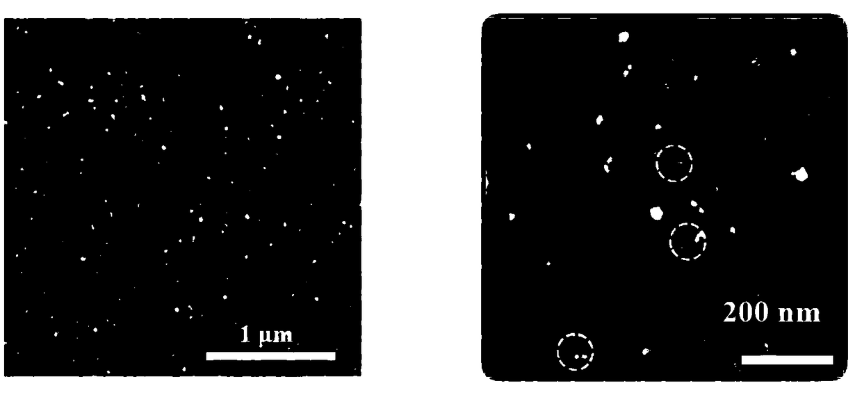
[0072] Such as Figure 4 a shows the atomic force scanning electron microscope image of the silk fibroin film doped with bovine serum of this embodiment and wrapped with gold nanoclusters, Figure 4 b for Figure 4 a Corresponding surface potential scans. Figure 5 for Figure 4 a and Figure 4 b Surface potenti...


PUM

PropertyMeasurementUnit
Thicknessaaaaaaaaaa
Thicknessaaaaaaaaaa
Sizeaaaaaaaaaa

Abstract

The invention provides a metal nano-cluster doped memristor and a method for preparing the same, and relates to the technical field of microelectronics. The metal nano-cluster doped memristor comprises an upper electrode, a resistance random layer and a lower electrode. The resistance random layer is positioned between the upper electrode and the lower electrode and is a thin film made from resistance random materials, and metal nano-clusters are doped in the thin film. The method includes S1, cleaning the lower electrodes; S2, forming the resistance random layer on a surface of the cleaned lower electrode in pulling film coating modes; S3, growing the upper electrode on the resistance random layer by the aid of magnetron sputtering processes. The metal nano-cluster doped memristor and themethod have the advantages that the metal nano-clusters are doped into thin film materials made from the resistance random materials to prepare corresponding metal nano-cluster doped composite thin films, effects of reinforcing local electric fields can be realized by the metal nano-clusters under the effects of electric fields, and the resistance transformation characteristics can be improved; the metal nano-cluster doped memristor is stable in resistance random memory property and high in switch speed, and a foundation can be laid for designing and further developing memristors.

Description

technical field [0001] The invention relates to the technical field of microelectronics, and in particular to a metal nano-cluster doped memristor and a preparation method thereof. Background technique [0002] Memristor utilizes two or more different resistive states exhibited by resistive layer materials under the action of an applied electric field to realize data storage. It is a new type of non-volatile memory that has been widely concerned in recent years. Initiate a research boom with academia. The memristor is composed of a simple upper electrode-resistive layer-bottom electrode sandwich structure, in which the material of the resistive layer is the carrier for the resistance transition of the memristor, and different types of resistive materials cause the memristor to present different storage windows. value, retention characteristics and erasing and writing speed, etc., and its performance parameters are closely related to the properties of the resistive layer mat...

Claims


Application Information

Patent Timeline
IPC IPC(8): H01L45/00B82Y30/00B82Y40/00
CPCB82Y30/00B82Y40/00H10N70/881H10N70/041
Inventor 刘向阳史晨阳
Owner XIAMEN UNIV
Why Eureka
Try Eureka