SiC knot barrier Schottky diode and manufacturing method thereof

A technology of junction barrier Schottky and manufacturing method, which is applied in the field of SiC junction barrier Schottky diodes and its manufacture, and can solve problems such as high diode conduction voltage, low electron penetration rate, and increased conduction resistance , to achieve the effect of accurately changing the effective barrier height

Inactive Publication Date: 2019-03-12
QINHUANGDAO JINGHE SCI & TECH RES INST CO LTD
View PDF3 Cites 2 Cited by
  • Summary
  • Abstract
  • Description
  • Claims
  • Application Information

AI Technical Summary

Problems solved by technology

Due to the limitation of the barrier height, the electron penetration rate is low, which is equivalent to increasing the on-resistance, so that the on-state voltage of the diode is higher

Method used


Image

  • SiC knot barrier Schottky diode and manufacturing method thereof
  • SiC knot barrier Schottky diode and manufacturing method thereof
  • SiC knot barrier Schottky diode and manufacturing method thereof

Examples


Embodiment 1

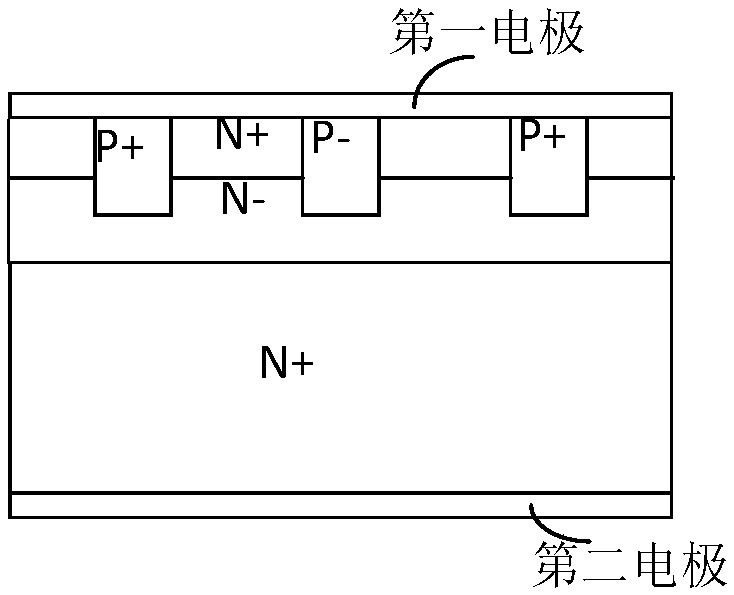
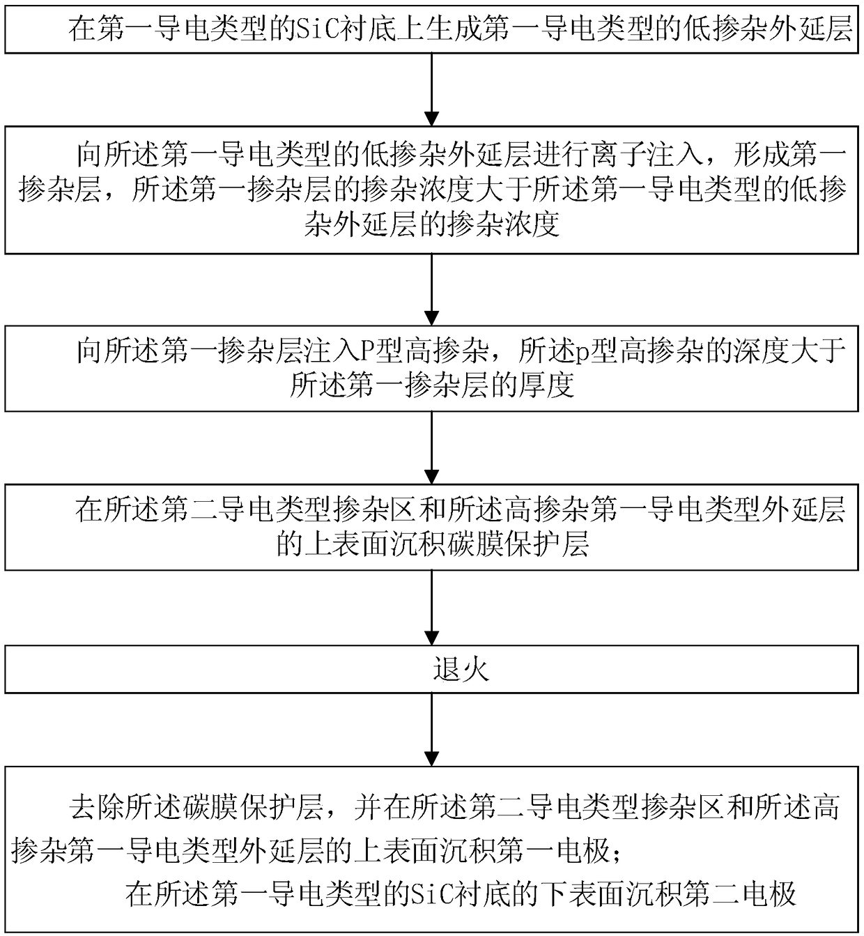
[0047] See attached picture, figure 1 Schematic diagram of the structure of the SiC junction barrier Schottky diode provided by the present invention; figure 2 A flow chart of the manufacturing method of the SiC junction barrier Schottky diode provided by the present invention; image 3 A flow chart of another manufacturing method of the SiC junction barrier Schottky diode provided by the present invention.

[0048] Usually a Schottky barrier is formed on a given semiconductor (such as n-type or p-type SiC), and there are only a limited number of barrier heights to choose from. Affected by the barrier height, the turn-on voltage of silicon carbide diodes is relatively large , in order to solve this technical problem, the present invention proposes an idea of ​​introducing a thin layer that can control the amount of impurities on the semiconductor surface, so that the effective barrier height of the metal-semiconductor contact can be changed, thereby reducing the conductivity...

Embodiment 2

[0055] On the basis of the above embodiments, this embodiment further details the internal structure of the SiC junction barrier Schottky diode:

[0056] Take the first conductivity type as P type and the second conductivity type as N type as an example:

[0057] The P-type SiC substrate layer includes a first surface and a second surface, the first surface is provided with a low-doped P-type epitaxial layer, and the doping concentration of the low-doped P-type epitaxial layer is 10 15 atom / cm 3 order of magnitude, the doping concentration of the low-doped P-type epitaxial layer is less than the doping concentration of the P-type SiC substrate layer; further, a highly-doped P-type epitaxial layer is set on the upper surface of the low-doped P-type The doping concentration of the hetero P-type epitaxial layer is 10 16 atom / cm 3 order, the highly doped P-type epitaxial layer is provided with multiple N-type doped regions, and the implantation concentration is 10 18 atom / cm ...

Embodiment 3

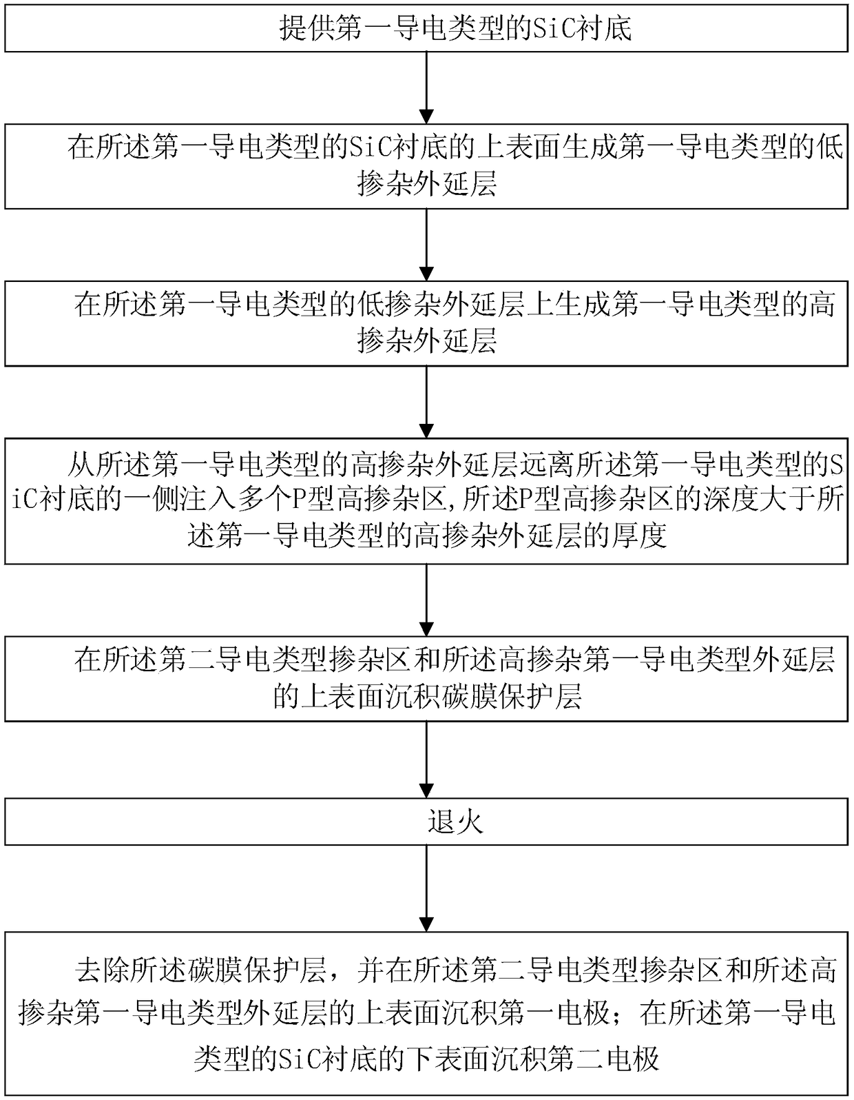
[0060] On the basis of the above embodiments, an embodiment of the present invention provides a method for manufacturing a SiC junction barrier Schottky diode, specifically:

[0061] Step 1: providing a SiC substrate of the first conductivity type;

[0062] Step 2: forming a low-doped epitaxial layer of the first conductivity type on the upper surface of the SiC substrate of the first conductivity type;

[0063] Step 3: generating a highly doped epitaxial layer of the first conductivity type on the lowly doped epitaxial layer of the first conductivity type;

[0064] Step 4: Implanting a plurality of P-type highly doped regions from the side of the highly doped epitaxial layer of the first conductivity type away from the SiC substrate of the first conductivity type, and the depth of the P-type highly doped regions is greater than the thickness of the highly doped epitaxial layer of the first conductivity type;

[0065] Step 5: Depositing a carbon film protective layer on the ...


PUM


Abstract

The invention relates to a SiC knot barrier Schottky diode and a manufacturing method thereof. The SiC knot barrier Schottky diode comprises a first conductive type SiC substrate layer, a low-doped first conductive type epitaxial layer, a high-doped first conductive type epitaxial layer, and multiple second conductive type doping areas; the depth of the second conductive type doping area is greater than the thickness of the high-doped first conductive type epitaxial layer, a first electrode and a second electrode. By adjusting the surface doping concentration, the barrier width is reduced, sothat the barrier of the diode is reduced, the effective barrier height of the contact of the metal-semiconductor is changed through different doping concentrations, the barrier width is reduced, and the electron with small free path can penetrate the barrier, the forward tunneling current is increased, the on-state resistance is equivalently reduced, and the diode breakover can be realized throughsmall voltage.

Description

technical field [0001] The invention belongs to the technical field of manufacturing methods of power devices, and in particular relates to a SiC junction barrier Schottky diode and a manufacturing method thereof. Background technique [0002] Silicon carbide metal oxide semiconductor field effect transistor (MOSFET) is a widely used silicon carbide power device. Wherein the control signal is supplied to a gate electrode which separates the semiconductor surface by an intervening insulator, such as silicon dioxide. Current conduction occurs by transport of majority carriers without the need for minority carrier injection as in bipolar transistor operation. SiC MOSFETs can provide a very large safe operating area, and multiple cell structures can be used in parallel. [0003] For an ideal Schottky barrier, the barrier height is determined by the properties of the metal and metal-semiconductor interface and has nothing to do with doping. Typically a Schottky barrier is form...

Claims


Application Information

Patent Timeline
Patent Type & Authority Applications(China)
IPC IPC(8): H01L29/06H01L29/872H01L21/329H01L21/04
CPCH01L21/0455H01L29/0684H01L29/6606H01L29/872
Inventor 邵锦文侯同晓孙致祥贾仁需元磊张秋洁刘学松
Owner QINHUANGDAO JINGHE SCI & TECH RES INST CO LTD
Why Eureka
Try Eureka