Organic compound and application thereof
A technology of organic compounds and mixtures, applied in the field of organic optoelectronic materials, to achieve the effect of improving exciton dispersion, improving luminescence performance and lifespan
- Summary
- Abstract
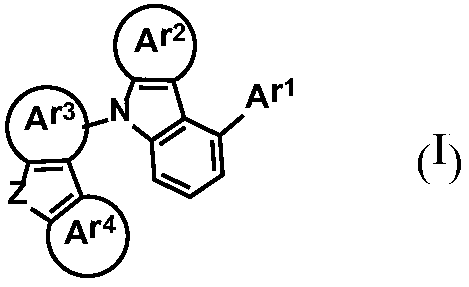
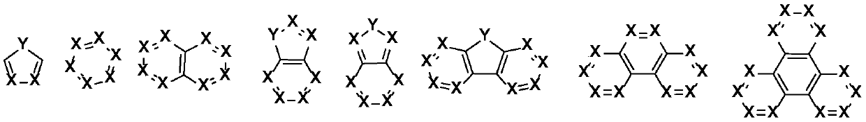
- Description
- Claims
- Application Information
AI Technical Summary
Problems solved by technology
Method used
Image

Examples
preparation example Construction
[0174] According to the above-mentioned preparation method, the thickness of the formed functional layer is 5nm-1000nm.
[0175] The present invention also provides an application of the above-mentioned organic compound, polymer, mixture or composition in an organic electronic device. The organic electronic device can be selected from, but not limited to, an organic light emitting diode (OLED), Organic Photovoltaics (OPV), Organic Light Emitting Cells (OLEEC), Organic Field Effect Transistors (OFETs), Organic Light Emitting Field Effect Transistors, Organic Lasers, Organic Spintronic Devices, Organic Sensors and Organic Plasmon Emitting Diodes (Organic Plasmon Emitting Diode) etc., particularly preferably OLED. In the embodiment of the present invention, the organic compound or high polymer is preferably used in the light-emitting layer of the OLED device.
[0176] The present invention further relates to an organic electronic device, comprising at least one organic compound,...
Embodiment 1
[0188] Embodiment 1: the synthesis of compound 1-3
[0189]
[0190] Synthesis of Intermediate 1-3-3
[0191] Under nitrogen atmosphere, (22.6g, 100mmol) compound 1-3-1, (19.8g, 100mmol) compound 1-3-2, (5.8g, 5mmol) Pd(PPh 3 ) 4, (6.4g, 20.0mmol) sodium carbonate, (1.8g, 5.64mmol) tetrabutylammonium bromide, 250mL 1,4-dioxane and 50mL water were added to a 500mL three-necked flask, heated at 80°C for 6 hours , after the reaction was completed, the reaction solution was inverted in 500 mL of pure water, the precipitated solid was suction-filtered, and the filter residue was purified by recrystallization to obtain intermediate 1-3-3 with a yield of 70%.
[0192] Synthesis of Intermediate 1-3-5
[0193] Under nitrogen atmosphere, (24.6g, 100.0mmol) compound 1-3-4, (38.1g, 150mmol) biboronic acid pinacol ester, (39.2g, 400mmol) potassium acetate, (3.66g, 5mmol) Pd (ppf )Cl 2 Add 250mL of 1,4-dioxane as a solvent into a 500mL three-neck flask, heat at 110°C for 12 hours, a...
Embodiment 2
[0198] Embodiment 2: the synthesis of compound 1-6
[0199]
[0200] Synthesis of Intermediate 1-6-2
[0201] Under nitrogen atmosphere, (17.5g, 60mmol) intermediate 1-3-5, (20.6g, 60mmol) intermediate 1-6-1, (2.08 g, 1.2mmol) tetrakistriphenylphosphine palladium, (12.7g , 120mmol) sodium carbonate, (3.9g, 12mmol) tetrabutylammonium bromide, 150mL of 1,4-dioxane and 30mL of water were added to a 500mL three-neck flask, heated at 80°C and stirred for 6 hours to end the reaction , the reaction solution was inverted in 500 mL of pure water, the precipitated solid was suction-filtered, and the filter residue was purified by recrystallization to obtain intermediate 1-6-2 with a yield of 70%.
[0202] Synthesis of compounds 1-6
[0203] Under nitrogen atmosphere, (9.48g, 20mmol) intermediate 1-6-3, (5g, 20mmol) compound 1-3-7, (1.91g, 10mmol) cuprous iodide, (2.28g, 20mmol) trans Cyclohexanediamine, (12.72g, 40mmol) potassium phosphate and 100mL toluene were added to a 300mL t...
PUM
| Property | Measurement | Unit |
|---|---|---|
| temperature | aaaaa | aaaaa |
| emission peak | aaaaa | aaaaa |
| glass transition temperature | aaaaa | aaaaa |
Abstract
Description
Claims
Application Information
 - R&D
- Intellectual Property
- Life Sciences
- Materials
- Tech Scout
- Unparalleled Data Quality
- Higher Quality Content
- 60% Fewer Hallucinations
Browse by: Latest US Patents, China's latest patents, Technical Efficacy Thesaurus, Application Domain, Technology Topic, Popular Technical Reports.
© 2025 PatSnap. All rights reserved.Legal|Privacy policy|Modern Slavery Act Transparency Statement|Sitemap|About US| Contact US: help@patsnap.com