A three-dimensional multilayer structure surface enhanced Raman substrate and its preparation method

A technology of structured surface and Raman substrate, which is applied in the field of molecular recognition to achieve the effect of good controllability and rich structure

Active Publication Date: 2021-11-02
BEIHUA UNIV
View PDF0 Cites 0 Cited by
  • Summary
  • Abstract
  • Description
  • Claims
  • Application Information

AI Technical Summary

Problems solved by technology

In addition, based on the research on SERS, people mainly focus on the surface plasmon resonance embodied by a single noble metal structure, but there are few studies on the surface plasmon resonance of the semiconductor-based metal composite structure system, although there are also studies on the metal-semiconductor. Composite structures are used as SERS substrates, but there are few reports on the composite structures of semiconductor + metal nanoparticles + dielectric layer + metal nanoparticles as SERS substrates.

Method used


Image

  • A three-dimensional multilayer structure surface enhanced Raman substrate and its preparation method
  • A three-dimensional multilayer structure surface enhanced Raman substrate and its preparation method
  • A three-dimensional multilayer structure surface enhanced Raman substrate and its preparation method

Examples


preparation example Construction

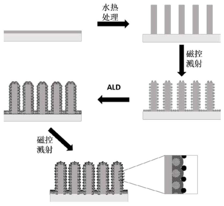
[0055] The present invention also provides a method for preparing a surface-enhanced Raman substrate with a three-dimensional multilayer structure, comprising the following steps:

[0056] Step 1, growing the ZnO seed layer:

[0057] The substrate was ultrasonically cleaned by acetone, ethanol, and deionized water for 10 minutes, and a ZnO seed layer was grown on the surface of the substrate by magnetron sputtering. The radio frequency power was 80W, the flow rate of argon gas was 40 sccm, and the growth time was 10 minutes;

[0058] Step 2, preparing ZnO nanorod arrays:

[0059] Zn(NO 3 ) 2 ·6H 2 O solution and C 6 h 12 N 4 The solutions are mixed, and the mixed solution is placed in a reaction kettle, and then the substrate for growing the ZnO seed layer is placed in the reaction kettle for reaction. The reaction temperature is 95° C. and the time is 3 hours. After the reaction is completed, the substrate is taken out. Wash it with deionized water and dry it to get a ...

Embodiment 1

[0070] 1. Grow ZnO seed layer: 1*1cm 2 The ITO substrate was ultrasonically cleaned with acetone, ethanol, and deionized water for 10 minutes, respectively. A ZnO thin film with a thickness of 15 nm was grown on the surface of the substrate by magnetron sputtering, the radio frequency power was 80 W, the flow rate of argon gas was 40 sccm, and the growth time was 10 min.

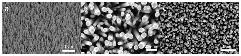
[0071] 2. Preparation of ZnO nanorod arrays: 0.025mol / L of Zn(NO 3 ) 2 ·6H 2 O (2.9749g) and 0.025mol / L of C 6 h 12 N 4 (1.419g) each took 10mL, mixed the above two solutions, and put them in the reaction kettle. Then, put the ITO conductive glass substrate coated with the seed layer solution vertically into it, react at 95°C for 3 hours, take out the substrate, clean it with deionized water, and dry it to get a neat substrate. ZnO nanorod arrays, see figure 2 a. From figure 2 a It can be seen that the nanorods grow perpendicular to the substrate and are uniformly arranged, with a diameter of 100...

Embodiment 2

[0079] 1. Grow ZnO seed layer: 1*1cm 2 The ITO substrate was ultrasonically cleaned with acetone, ethanol, and deionized water for 10 minutes, respectively. A ZnO thin film with a thickness of 15 nm was grown on the surface of the substrate by magnetron sputtering, the radio frequency power was 80 W, the flow rate of argon gas was 40 sccm, and the growth time was 10 min.

[0080] 2. Preparation of ZnO nanorod arrays: 0.025mol / L of Zn(NO 3 ) 2 ·6H 2 O (2.9749g) and 0.025mol / L of C 6 h 12 N 4(1.419g) each took 10mL, mixed the above two solutions, and put them in the reaction kettle. Then, put the ITO conductive glass substrate coated with the seed layer solution vertically into it, react at 95°C for 3 hours, take out the substrate, clean it with deionized water, and dry it to get a neat substrate. The ZnO nanorod array, the nanorods grow perpendicular to the substrate, are uniformly arranged, have a diameter of 100nm, and a length of 1μm.

[0081] 3. Preparation of ZnO@A...


PUM

PropertyMeasurementUnit
thicknessaaaaaaaaaa
thicknessaaaaaaaaaa
thicknessaaaaaaaaaa

Abstract

The invention belongs to the technical field of molecular recognition, and in particular relates to a surface-enhanced Raman substrate with a three-dimensional multilayer structure and a preparation method thereof. The surface-enhanced Raman substrate of the three-dimensional multilayer structure of the present invention comprises: a substrate; a ZnO seed layer grown on the surface of the substrate; a ZnO nanorod array grown on the ZnO seed layer; coated on the ZnO nanorod array Ag nanoparticle layer on the surface; Al grown on the surface of the ZnO nanorod array structure covered by the Ag nanoparticle layer 2 o 3 dielectric layer; deposited on the Al 2 o 3 Ag nanoparticles layer on dielectric layer. The present invention adopts the combination method of chemical method, magnetron sputtering and atomic layer deposition technology to prepare a new type of composite structure SERS substrate, the substrate structure includes a three-dimensional structure of the substrate, a core-shell structure, a sandwich structure, etc. SERS substrates with variable and rich structures are of great significance for the study of multiple SERS mechanisms and the expansion of SERS applications.

Description

technical field [0001] The invention belongs to the technical field of molecular recognition, and in particular relates to a surface-enhanced Raman substrate with a three-dimensional multilayer structure and a preparation method thereof. The substrate prepared by the method can be applied to a surface-enhanced Raman scattering substrate. Background technique [0002] Surface plasmon resonance is a phenomenon in which metal nanostructures interact with free electrons on the metal surface under light to generate related resonances. It has attracted much attention because of its unique optical properties at the nanoscale. / Metal oxide multilayer nanostructure and optical vector field on surface plasmon regulation will produce surface Raman enhancement, transmission enhancement, nonlinear optical enhancement, semiconductor carrier radiation recombination speed enhancement, luminous efficiency enhancement, A series of novel effects such as photocatalytic enhancement have attracte...

Claims


Application Information

Patent Timeline
Patent Type & Authority Patents(China)
IPC IPC(8): G01N21/65
CPCG01N21/658
Inventor 牟佳佳孙伟杰郝婷婷
Owner BEIHUA UNIV
Why Eureka
Try Eureka