

Grinding solution and preparation method thereof
A technology of grinding liquid and grinding sand, which is applied in chemical instruments and methods, and other chemical processes, can solve the problems of difficulty in ensuring the grinding quality of the grinding object and the decrease of grinding efficiency with the grinding time, so as to maintain the grinding efficiency and not reduce the efficiency Effect
- Summary
- Abstract
- Description
- Claims
- Application Information
AI Technical Summary
Problems solved by technology
Method used
Image

Examples
preparation example Construction
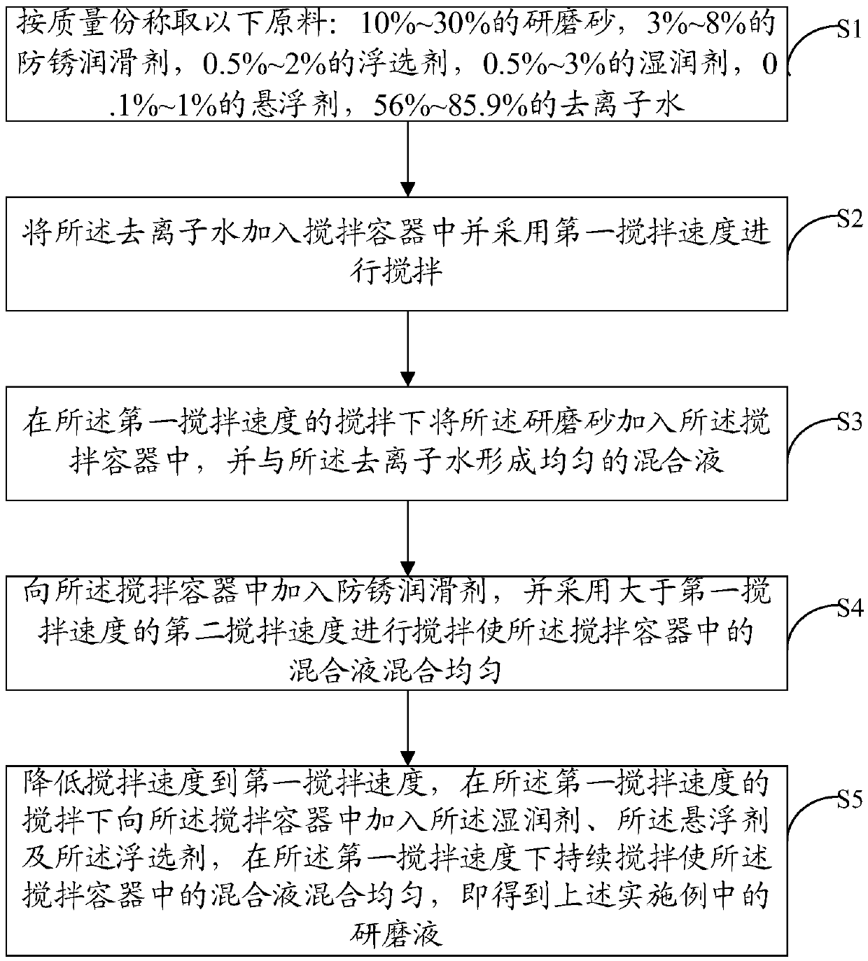
[0029] The invention also discloses a preparation method of grinding liquid, please refer to figure 1 , including the following steps:
[0030] S1. Weigh the following raw materials in parts by mass: 10% to 30% of grinding sand, 3% to 8% of antirust lubricant, 0.5% to 2% of flotation agent, 0.5% to 3% of wetting agent, 0.1 %~1% suspending agent, 56%~85.9% deionized water;
[0031] S2. Add the deionized water into the stirring container and stir at the first stirring speed; of course, the above-mentioned stirring container is preferably a stirring tank, and can also be a stirring container of other shapes, such as a stirring tank, a stirring bucket, a beaker, a flask Wait.
[0032] S3. Add the grinding sand into the stirring container under stirring at the first stirring speed, and form a uniform mixed solution with the deionized water;
[0033] S4. Add an anti-rust lubricant into the stirring container, and stir at a second stirring speed higher than the first stirring spee...
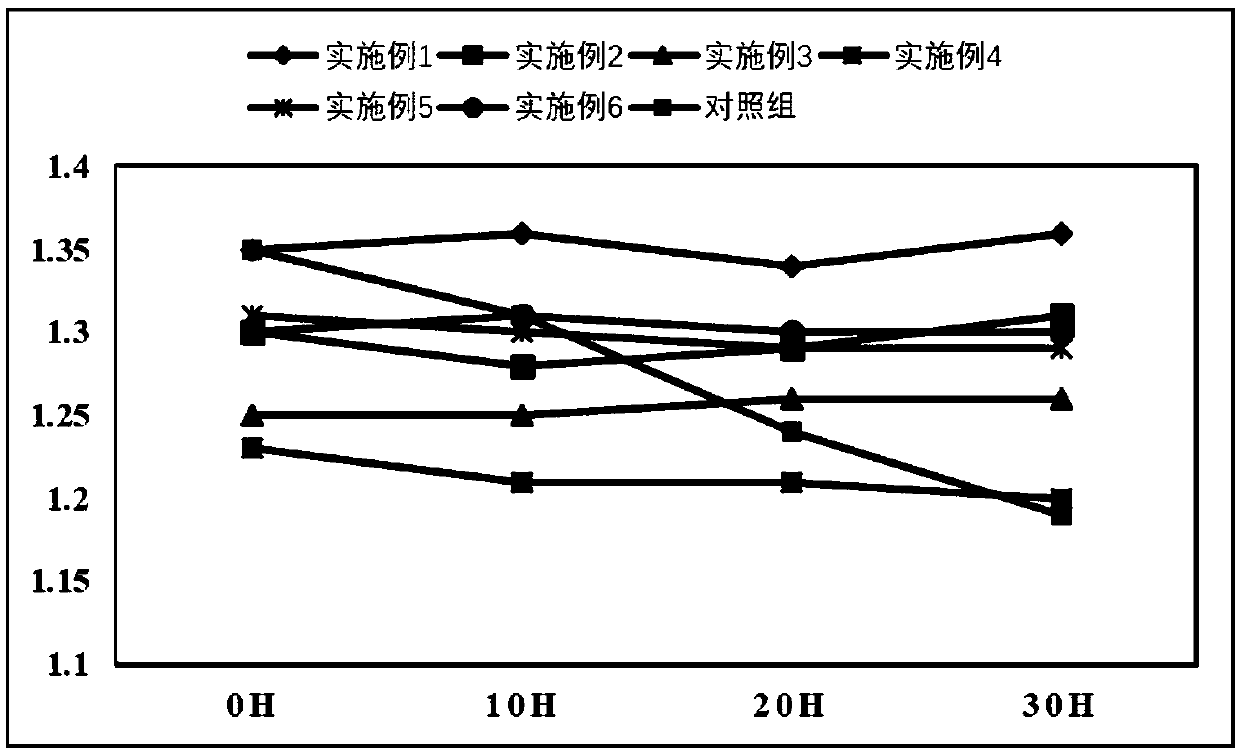
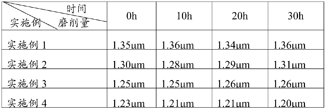
Embodiment 1
[0036] The embodiment of the present invention provides a grinding liquid, which is used in the process of batch processing of new silicon wafers or silicon wafers. The grinding liquid includes the following raw materials in parts by mass: 10% grinding sand, 3% anti-rust lubricant Agent, 0.5% flotation agent, 0.5% wetting agent, 0.1% suspending agent, 89.5% deionized water.
[0037] Wherein, the abrasive sand is silicon carbide with a particle size of 3-4 μm, the anti-rust lubricant is monoethanolamine ammonium borate, the flotation agent is octadecyl primary amine, and the wetting agent is sulfonated succinate Acid dioctyl sodium salt, the suspending agent is sodium carboxymethylcellulose.
[0038]The preparation method of described grinding liquid in the present embodiment, comprises the steps:
[0039] (1) Weigh the following raw materials in parts by mass: 10% silicon carbide with a particle size of 3 to 4 μm, 3% monoethanolamine ammonium borate, 0.5% octadecyl primary am...
Embodiment 2
[0045] The embodiment of the present invention provides a kind of grinding liquid, is used in the process of batch processing of novel silicon wafer or silicon wafer, and described grinding liquid comprises the raw material of following mass parts: 30% grinding sand, 8% antirust lubricating Agent, 2% flotation agent, 3% wetting agent, 1% suspending agent, 56% deionized water.
[0046] Wherein, the grinding sand is 4000 mesh alumina, the anti-rust lubricant is triethanolamine carboxylate, and the flotation agent is polyacrylamide; the wetting agent is polyoxyethylene ether glyceride and glycerin and The mixture of sorbitol, the mass ratio of polyoxyethylene ether glyceride to glycerin and sorbitol is 1:1:1; the suspending agent is sodium tripolyphosphate.
[0047] The preparation method of described grinding liquid in the present embodiment, comprises the steps:
[0048] (1) Take the following raw materials by mass parts: 30% of 4000 mesh alumina, 8% of triethanolamine carboxy...
PUM
| Property | Measurement | Unit |
|---|---|---|
| particle diameter | aaaaa | aaaaa |
Abstract
Description
Claims
Application Information