Organic thin film transistor and preparation method thereof

An organic thin film and transistor technology, applied in the field of organic thin film transistors and their preparation, can solve problems such as damage to the surface of a flat layer, and achieve the effects of increasing carrier mobility, reducing production costs, and improving manufacturing efficiency

Inactive Publication Date: 2019-04-30
NINGBO GRAPHENE INNOVATION CENT CO LTD
View PDF5 Cites 1 Cited by
  • Summary
  • Abstract
  • Description
  • Claims
  • Application Information

AI Technical Summary

Problems solved by technology

[0003] The inventors found that the above method has at least the following problems: the flat layer usually requires high-energy ultraviolet curing and high temperature and long-term thermal curing to obtain a highly cross-linked insulating film
[0006] In the process of removing photoresist, in order to remove the residual photoresist in the channel as much as possible and realize high-quality electrode layer production, multiple processes of exposure and development are usually required, but too much developer flushing will also affect the process to a certain extent. upper damage planar surface

Method used


Image

  • Organic thin film transistor and preparation method thereof
  • Organic thin film transistor and preparation method thereof
  • Organic thin film transistor and preparation method thereof

Examples


preparation example Construction

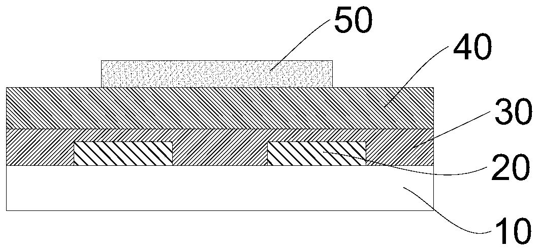
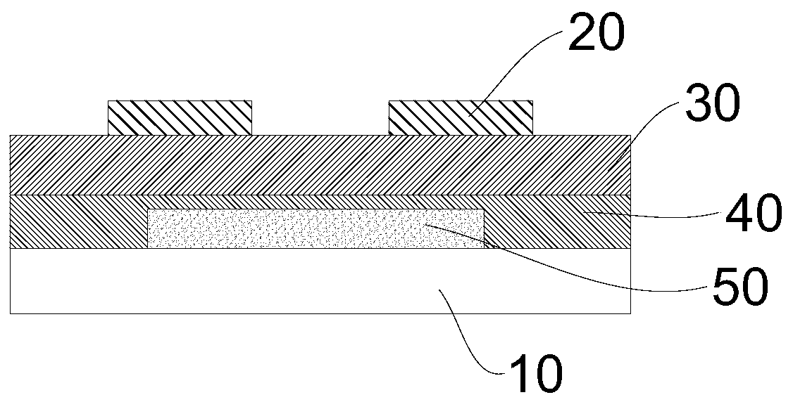
[0039] Organic thin film transistor (wherein, the electrode layer close to substrate 10 is source drain layer 20, refer to figure 1 ) preparation method, comprising the steps of:

[0040] (1) Select the substrate 10 , such as a glass substrate, a silicon substrate or a flexible substrate. Among them, the flexible substrate can be: PI (polyimide) substrate, PET (polyethylene terephthalate) substrate, PEN (polyethylene naphthalate) substrate, PES (polyethersulfone) substrate , PC (polycarbonate) substrate, PVA (polyvinyl alcohol) substrate, PP (polypropylene) substrate, MYLAR film substrate, PEEK (polyether ether ketone) substrate, PPA (polyparaphenylene terephthalamide) substrate , PTFE (polytetrafluoroethylene) substrate, PMMA (polymethyl methacrylate) substrate, PDMS (polydimethylsiloxane) substrate, etc.

[0041] In this embodiment, the shape and thickness of the substrate 10 are not limited, as long as the organic thin film transistor can be prepared. Furthermore, if the...
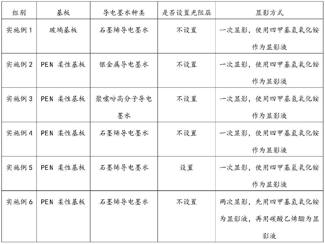
Embodiment 1

[0077] The comparison between Example 1 and Example 4 shows that compared with the glass substrate, the electrical performance of the organic thin film transistor obtained by coating the graphene conductive ink on the PEN flexible substrate is better.

Embodiment 2

[0078] Embodiment 2, embodiment 3 and embodiment 4 compare illustration, compare with silver metal conductive ink and polythiophene polymer conductive ink, on PEN flexible substrate, coat graphene conductive ink, the electrical performance of the organic thin film transistor that obtains better.


PUM


Abstract

The invention provides an organic thin film transistor and a preparation method thereof, which belong to the technical fields of organic electronics and photo-electronics. The organic thin film transistor includes a substrate, a source-drain layer containing a source and a drain, an organic semiconductor layer, a gate insulating layer and a gate layer. One surface of the substrate is the source-drain layer. The surface of the source-drain layer away from the substrate is the organic semiconductor layer. The surface of the organic semiconductor layer away from the source-drain layer is the gateinsulating layer. The surface of the gate insulating layer away from the organic semiconductor layer is the gate layer. The source-drain layer is made of conductive ink. The preparation method of theorganic thin film transistor includes the following steps: coating one surface of a substrate with conductive ink; curing the conductive ink to form a first electrode layer; and exposing, developingand heat-treating the first electrode layer to obtain a source-drain layer. The organic thin film transistor prepared by the method needs neither a flat layer nor a photoresist layer, and can be patterned directly.

Description

technical field [0001] The invention relates to the technical fields of organic electronics and optoelectronics, in particular to an organic thin film transistor and a preparation method thereof. Background technique [0002] In the prior art, the preparation method of an organic thin film transistor is usually to form an organic planar layer on the substrate, and then deposit metal or metal alloy on the organic planar layer to form an electrode layer, which can be a gate layer, or form a source layer and a drain layer. polar layer. [0003] The inventors found that the above method has at least the following problems: the planar layer usually requires high-energy ultraviolet curing and high-temperature, long-time thermal curing to obtain a highly cross-linked insulating film. The manufacturing process is complicated, which increases the production cost and reduces the manufacturing efficiency of the device substrate. [0004] When depositing metal or metal alloy on a flat...

Claims


Application Information

Patent Timeline
Patent Type & Authority Applications(China)
IPC IPC(8): H01L51/10H01L51/05H01L51/40
CPCH10K71/12H10K71/621H10K10/46H10K10/481H10K10/464H10K10/82H10K10/84
Inventor 卢珂鑫张燕红李伟伟谷文翠刘兆平
Owner NINGBO GRAPHENE INNOVATION CENT CO LTD
Why Eureka
Try Eureka