

MEMS device, preparation method and electronic device
A technology for electronic devices and devices, used in the manufacture of microstructure devices, measurement devices, electrical solid devices, etc., can solve the problems of poor interconnection layer bonding performance, affecting device performance and yield, etc., to solve bonding failures and improve performance. and yield effect
- Summary
- Abstract
- Description
- Claims
- Application Information
AI Technical Summary
Problems solved by technology
Method used
Image

Examples
preparation example Construction
[0067] In addition, the application also discloses a method for preparing a MEMS device, the method comprising:
[0068] form the backplane;
[0069] on the backplane;
[0070] Wherein, the interconnection layer includes a first conductive layer and a second conductive layer, and the interconnection layer further includes a diffusion barrier layer, and the diffusion barrier layer is arranged between the first conductive layer and the second conductive layer space, used to prevent the diffusion of the first conductive layer.
[0071] The present application provides a MEMS device and its preparation method. In the MEMS device, the interconnection layer includes a first conductive layer and a second conductive layer, and the interconnection layer also includes a diffusion barrier layer, and the diffusion barrier A layer is disposed between the first conductive layer and the second conductive layer for preventing diffusion of the first conductive layer. The present invention p...
Embodiment 1
[0073] Refer below figure 2 with Figures 3A-3E The preparation method of the MEMS device of the present invention is described in detail, figure 2 A flow chart of the fabrication process of the MEMS device of the present invention is shown; Figures 3A-3E The structure of a MEMS device in an embodiment of the present invention is shown.
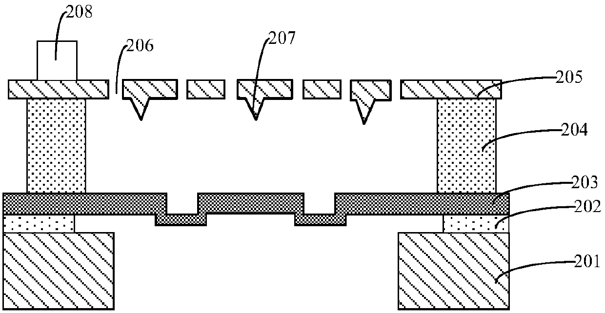
[0074] Such as Figure 3A Shown, described MEMS device in the present invention comprises:
[0075] Backplane 305;
[0076] an interconnection layer 308 on the backplane;
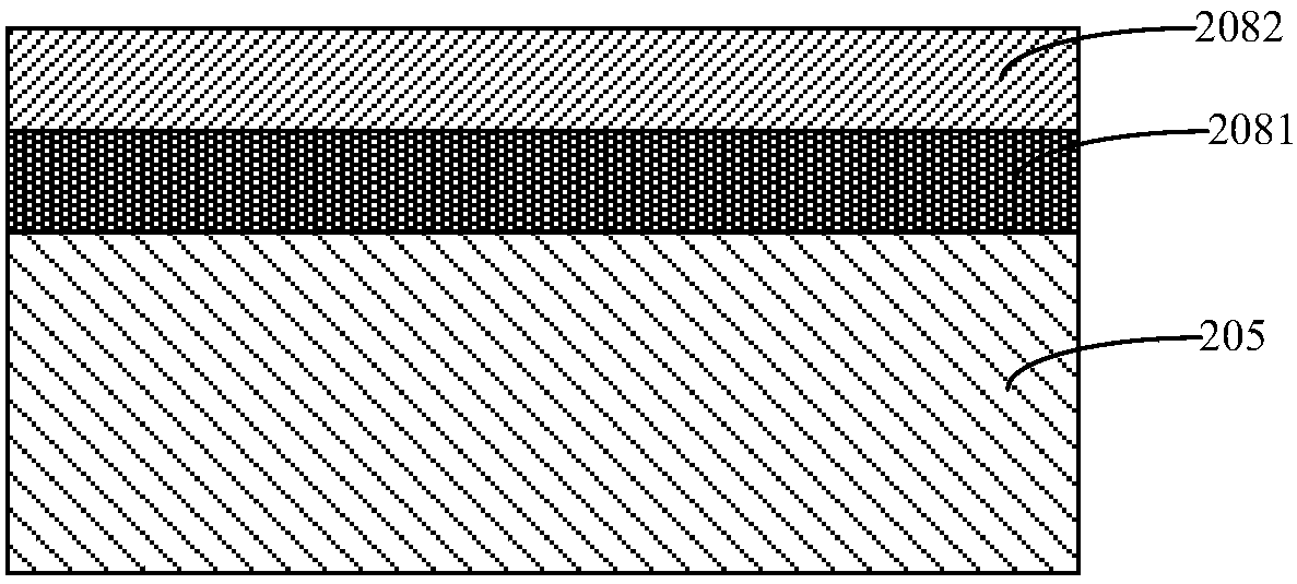
[0077] Wherein, the interconnection layer includes a first conductive layer and a second conductive layer, and the interconnection layer further includes a diffusion barrier layer 3082, and the diffusion barrier layer is arranged on the first conductive layer and the second conductive layer Between, used to prevent the mutual diffusion between the first conductive layer and the second conductive layer.
[0078] The interconnection layer serves as an interconnecti...
Embodiment 2
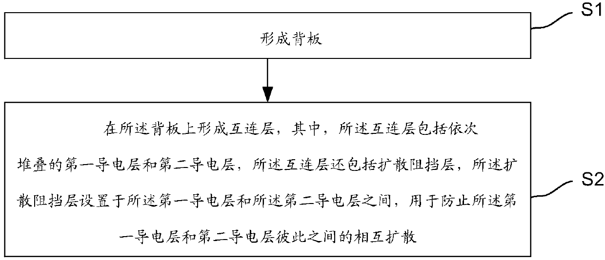
[0110] The present invention also provides a method for preparing a MEMS device, such as figure 2 As shown, the main steps of the preparation method include:
[0111] Step S1: forming a backplane;
[0112] Step S2: forming an interconnection layer on the backplane, wherein the interconnection layer includes a stacked first conductive layer and a second conductive layer, and the interconnection layer further includes a diffusion barrier layer, and the diffusion barrier layer It is arranged between the first conductive layer and the second conductive layer, and is used to prevent mutual diffusion between the first conductive layer and the second conductive layer.
[0113] The application provides a method for preparing a MEMS device, in which the interconnection layer includes a first conductive layer and a second conductive layer, the interconnection layer also includes a diffusion barrier layer, and the diffusion barrier layer It is arranged between the first conductive lay...
PUM
| Property | Measurement | Unit |
|---|---|---|
| Thickness | aaaaa | aaaaa |
| Thickness | aaaaa | aaaaa |
| Thickness | aaaaa | aaaaa |
Abstract
Description
Claims
Application Information