Selective emitter, preparation method thereof, solar cell using selective emitter, and application of solar cell

A solar cell and emitter technology, which is applied in the field of solar cells, can solve the problems of poor selective emitter effect, light conversion efficiency to be improved, and low diffusion square resistance of silicon wafers, so as to improve photoelectric conversion efficiency and short-circuit current and conversion efficiency, low-cost effect

Active Publication Date: 2019-05-03
YANCHENG CANADIAN SOLAR INC +1
View PDF7 Cites 3 Cited by
  • Summary
  • Abstract
  • Description
  • Claims
  • Application Information

AI Technical Summary

Problems solved by technology

When lightly doped, the central square resistance is different from the edge square resistance, which leads to the difference between the lightly doped square resistance and the heavily doped square resistance in the central area of ​​the silicon wafer is much larger than that of the edge area, which will lead to selectivity. The effect of the emitter preparation is not good
[0004] CN102738258A discloses a laser-doped selective emitter solar cell, which includes a battery body, which is a silicon wafer layer, and is characterized in that a positive electrode layer is distributed at the bottom of the silicon wafer layer, and a positive electrode layer is arranged on the top of the silicon wafer layer. Diffusion-doped mixed layer, and the back electrode is distributed on the diffused-doped mixed layer; the finished silicon wafer of this invention has low diffusion square resistance and good uniformity, which can increase the light conversion efficiency of the cell, but its cost is high, and it is not suitable for Industrial application
[0005] CN103367124A discloses a method for making a selective emitter battery, comprising the steps of: 1) removing the damaged layer of the silicon wafer, and preparing a textured surface on the surface of the silicon wafer; 2) removing the damaged layer and preparing the textured surface of the silicon wafer Spray phosphorus source and laser doping; 3) Perform high-temperature chain diffusion on silicon wafers sprayed with phosphorus source and laser doping to obtain p-n junctions in areas other than the front positive electrode area; 4) Remove silicon wafers that have undergone high-temperature chain diffusion PSG on the surface and the p-n junction on the periphery; 5) Deposit a layer of silicon nitride film on the surface of the silicon wafer after removing the PSG on the surface and the p-n junction on the periphery; 6) On the silicon nitride film with the silicon nitride film Print the back electrode, the back electric field and the positive electrode on the chip, and carry out sintering, make the electrode metallization, obtain the selective emitter battery; 7) test the various parameters of the selective emitter battery, and classify it according to the process standard; but Its light conversion efficiency still needs to be improved
The present invention carries out two modification methods to the existing SE technology laser MARK point, wherein the laser marking energy of the new MARK point in the laser process is higher than the energy of the laser doped line, so that the chromaticity and There is a significant difference between the shape and the non-laser area; at the same time, the square MARK point is printed with a square laser spot to eliminate edge irregularities, which is convenient for the naked eye to confirm whether the offset exceeds the standard and the direction of the offset after the machine is printed. It is very worth promoting; but Its light conversion efficiency still needs to be improved

Method used


Image

  • Selective emitter, preparation method thereof, solar cell using selective emitter, and application of solar cell
  • Selective emitter, preparation method thereof, solar cell using selective emitter, and application of solar cell
  • Selective emitter, preparation method thereof, solar cell using selective emitter, and application of solar cell

Examples


Embodiment 1

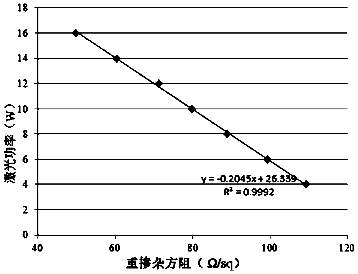
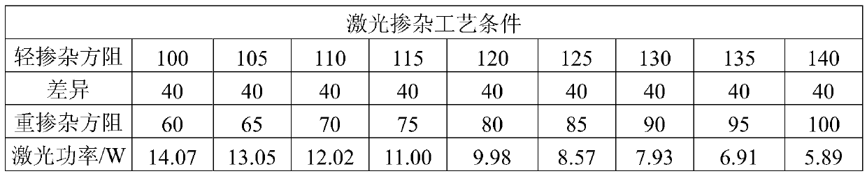
[0041] This embodiment provides a selective emitter, the difference between the lightly doped square resistance of the light receiving region of the selective emitter and the heavily doped square resistance of the non-light receiving region is a fixed value, and the fixed value is 40Ω / sq; where the light doping is tubular diffusion, and the heavy doping is laser doping.

[0042] The preparation method of the selective emitter is as follows:

[0043] (1) Remove the damaged sheet from the silicon wafer, prepare the suede surface, and obtain the pretreated silicon wafer, and then put the pretreated silicon wafer under the condition that the gas is a combination of oxygen, nitrogen and phosphorus oxychloride, and the temperature is 800 ° C. Carry out tubular diffusion, the time of tubular diffusion is 1000s, and obtain a lightly doped silicon wafer with a square resistance of 120±20Ω / sq, wherein during the light doping process, phosphorus oxychloride is carried into the diffusion...

Embodiment 2

[0052] This embodiment provides a selective emitter, the difference between the lightly doped square resistance of the light-receiving region of the selective emitter and the heavily doped square resistance of the non-light-receiving region is a fixed value, and the fixed value is 30Ω / sq; where the light doping is tubular diffusion, and the heavy doping is laser doping.

[0053] The preparation method of the selective emitter is as follows:

[0054] (1) Remove the damaged sheet from the silicon wafer, prepare the suede surface, and obtain the pretreated silicon wafer, and then put the pretreated silicon wafer under the condition that the gas is a combination of oxygen, nitrogen and phosphorus oxychloride, and the temperature is 760 ° C. Carry out tubular diffusion, the time of tubular diffusion is 1200s, and obtain a lightly doped silicon wafer with a square resistance of 120±20Ω / sq, wherein during the light doping process, phosphorus oxychloride is carried into the diffusion...

Embodiment 3

[0061] This embodiment provides a selective emitter, the difference between the lightly doped square resistance of the light receiving region of the selective emitter and the heavily doped square resistance of the non-light receiving region is a fixed value, and the fixed value is 50Ω / sq; where the light doping is tubular diffusion, and the heavy doping is laser doping.

[0062] The preparation method of the selective emitter is as follows:

[0063] (1) Remove the damaged sheet from the silicon wafer, prepare the textured surface, and obtain the pretreated silicon wafer, and then put the pretreated silicon wafer under the condition that the gas is a combination of oxygen, nitrogen and phosphorus oxychloride, and the temperature is 840 ° C. Carry out tubular diffusion, the time of tubular diffusion is 600s, and obtain a lightly doped silicon wafer with a square resistance of 120±20Ω / sq, wherein during the light doping process, phosphorus oxychloride is carried into the diffusi...


PUM


Abstract

The invention provides a selective emitter, a preparation method of the selective emitter, a solar cell using the selective emitter and an application of the solar cell. The difference between lightly-doped sheet resistance of a light receiving region and heavily-doped sheet resistance of a non-light receiving region of the selective emitter is a fixed value, and the fixed value is 40 + / -10 ohm / sq. The open-circuit voltage and the short-circuit current can be improved and the dead layer effect can be reduced by preparing the selective emitter, so that the light conversion efficiency is improved. The preparation method of the selective emitter is low in price, high in yield, simple in process condition, easy to operate and suitable for industrial large-scale production application. The prepared solar cell has high light conversion efficiency, greatly reduces the production cost, and can be applied to the field of photovoltaics as an energy cell.

Description

technical field [0001] The invention belongs to the field of solar cells, and relates to a selective emitter, its preparation method, a solar cell using it and its application. Background technique [0002] Selective emitter is a diffusion technology that heavily doped in the metal electrode area and lightly doped in the non-metal area, which can not only ensure the silver-silicon contact but also increase the minority carrier lifetime. In the diffusion process, in the process of doping phosphorus atoms to prepare the emitter, lighter doping can reduce minority carrier recombination and increase minority carrier lifetime, but lighter doping leads to poor contact of metal electrodes with silver and silicon, and increased contact resistance. Laser Doped Selective Emitter (LDSE) uses a laser beam to selectively irradiate the silicon surface to make the silicon substrate into a molten state, and the dopant atoms can quickly enter the molten silicon. When the laser beam disappear...

Claims


Application Information

Patent Timeline
Patent Type & Authority Applications(China)
IPC IPC(8): H01L31/0352H01L31/0216H01L31/06
CPCY02E10/50
Inventor 刘志强袁中存费正洪
Owner YANCHENG CANADIAN SOLAR INC
Why Eureka
Try Eureka