Method for manufacturing magnetic random access memory cell array and peripheral circuit connection line

A random access memory and cell array technology, applied in the manufacture/processing of electromagnetic devices, circuits, parts of electromagnetic equipment, etc., can solve problems such as time-dependent dielectric breakdown, damage diffusion barrier, damage, etc., to reduce complexity And the effect of production cost, electrical performance and yield improvement

Inactive Publication Date: 2019-05-03
SHANGHAI CIYU INFORMATION TECH CO LTD
View PDF4 Cites 7 Cited by
  • Summary
  • Abstract
  • Description
  • Claims
  • Application Information

AI Technical Summary

Problems solved by technology

However, since the size of the MTJ structural unit is smaller than that of the VIA x (x>=1) The size of the top opening is small. When etching the magnetic tunnel junction and its bottom electrode, in order to completely isolate the MTJ units, over-etching must be carried out. In the over-etching, the magnetic tunnel junction is not blocked. and its bottom electrode covered copper VIA x (x>=1) area will be partially etched, and also damage its diffusion barrier layer (Ta / TaN), which will form copper VIA x (x>=1) to the diffusion channel of the low-k dielectric outside it, Cu atom will be diffused in the low-k dielectric, and this is bound to affect the electrical performance of MRAM, such as: time-dependent dielectric breakdown (TDDB , Time Dependent DielectricBreakdown) and electron mobility (EM, Electron Mobility), etc., causing damage
[0007] In addition, during the over-etching process of the magnetic tunnel junction and its bottom electrode, due to ion bombardment (IonBombardment), copper atoms and their forming compounds will be sputtered to the sidewall of the magnetic tunnel junction and the etched low-k material surface, thereby contaminating the entire MRAM device

Method used


Image

  • Method for manufacturing magnetic random access memory cell array and peripheral circuit connection line
  • Method for manufacturing magnetic random access memory cell array and peripheral circuit connection line
  • Method for manufacturing magnetic random access memory cell array and peripheral circuit connection line

Examples


Embodiment example 1

[0062] Implementation case 1: two single damascene (SD, Single Damascene) processes, the steps are as follows:

[0063] Step 4.1.1: On the magnetic tunnel junction dielectric layer 304, deposit the top electrode through hole dielectric 401 and fill the dummy magnetic tunnel junction (Dummy-MTJ) opening 306, and finally, use the planarization process to grind the top electrode through hole ( TEV) dielectric 401, as shown in Figure 4(a); the top electrode via (TEV) dielectric 401 is SiO 2 , SiON or low-k and other materials, the thickness of which is 120nm ~ 400nm.

[0064] Step 4.1.2: Graphically define and form a top electrode through hole (TEV) 4021 and a top electrode through hole 4022 by an etching process. In the logic area, it is connected to the bottom electrode to contact the metal layer 301, and the process parameters are strictly controlled to keep a sufficient distance between the top electrode through hole (TEV) 4022 and the side wall of the dummy magnetic tunnel j...

Embodiment example 2

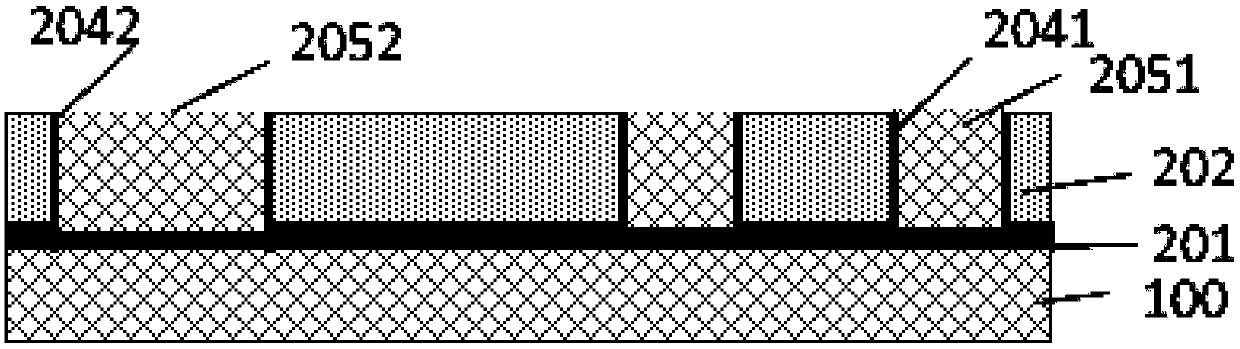
[0068] Implementation Case 2: Single Dual Damascene (DD, Dual Damascene) process, such as Figure 5 shown; the steps are as follows:

[0069] Step 4.2.1: On the magnetic tunnel junction dielectric layer 304, deposit the top electrode through hole dielectric 401 and fill the dummy magnetic tunnel junction (Dummy-MTJ) opening 306, and then use the planarization process to grind the top electrode through hole ( TEV) dielectric 401; top electrode via (TEV) dielectric 401 is SiO 2 , SiON or low-k and other materials, the thickness of which is 120nm ~ 400nm; finally, deposit metal wiring (M x+1 ) The thickness of the dielectric 406 is 50nm-300nm, and its material is SiO 2 , SiON or low-k, etc., usually before deposition, an etch barrier layer 405 with a thickness of tens of nanometers is deposited, and its material is SiN, SiC or SiCN, etc.;

[0070] Step 4.2.2: Graphically define and use an etching process to form the top electrode through hole (TEV) and the metal wiring groove ...


PUM


Abstract

The invention provides a method for manufacturing a magnetic random access memory cell array and a peripheral circuit connection line, comprising the steps of: (1) providing a surface-polished CMOS substrate having a metal connection line, fabricating a bottom electrode via on the substrate, and then filling the bottom electrode via with metal copper; (2) depositing a bottom electrode contact anda magnetic tunnel junction multilayer film on the bottom electrode via, fabricating a memory region bottom electrode contact and a magnetic tunnel junction memory cell array, and fabricating a logic region bottom electrode contact and a dummy magnetic tunnel junction (dummy-MTJ) unit; (3) fabricating a dummy magnetic tunnel junction opening in a logic region; and (4) fabricating a top electrode via and a copper metal connection line connecting the logic unit with the memory unit. A layer of bottom electrode contact is added under the magnetic tunnel junction so as to avoid the direct adjacencyof a CMOS back-end copper via and the etching process in the fabrication of the magnetic tunnel junction array, which is beneficial to the improvement in the electrical performance and yield of the devices.

Description

technical field [0001] The invention relates to a manufacturing method of a magnetic random access memory (MRAM) unit array and peripheral circuit wiring, and belongs to the technical field of magnetic random access memory (MRAM, Magnetic Radom Access Memory) manufacturing. Background technique [0002] In recent years, MRAM using Magnetic Tunnel Junction (MTJ) is considered to be the future solid-state non-volatile memory, which has the characteristics of high-speed reading and writing, large capacity and low energy consumption. Ferromagnetic MTJ is usually a sandwich structure, which has a magnetic memory layer, which can change the magnetization direction to record different data; an insulating tunnel barrier layer in the middle; a magnetic reference layer, located on the other side of the tunnel barrier layer, which The direction of magnetization remains unchanged. [0003] In order to record information in this magnetoresistive element, it is suggested to use a writing...

Claims


Application Information

Patent Timeline
Patent Type & Authority Applications(China)
IPC IPC(8): H01L43/12H01L43/02H01L27/22
Inventor 肖荣福张云森郭一民陈峻
Owner SHANGHAI CIYU INFORMATION TECH CO LTD
Why Eureka
Try Eureka