A graphene strip with neat edges, its preparation method and application
A graphene and edge technology, which is applied in the field of graphene strip preparation, can solve the problems of uneven strip edges, uncontrollable width, complicated process, etc., and achieves the advantages of reducing scattering, maintaining intrinsic properties, and simple process operation. Effect
- Summary
- Abstract
- Description
- Claims
- Application Information
AI Technical Summary
Problems solved by technology
Method used
Image
Examples
preparation example Construction
[0023] As an aspect of the technical solution of the present invention, a method for preparing a graphene strip with neat edges, which it relates to, includes:
[0024] Photolithographic patterning of graphene;
[0025] growing a metal film on the patterned graphene, after which the metal film is removed;
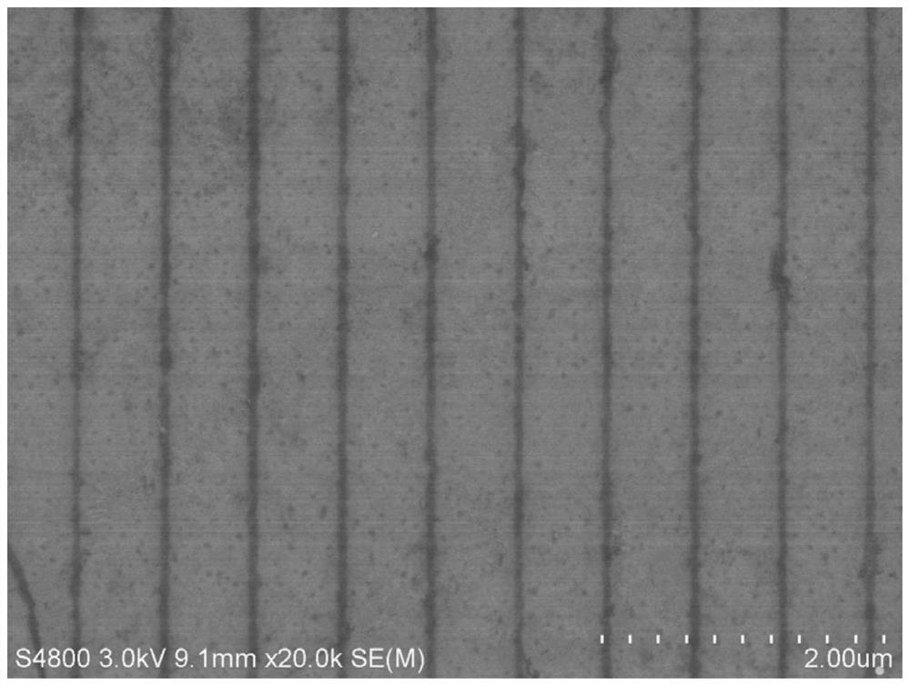
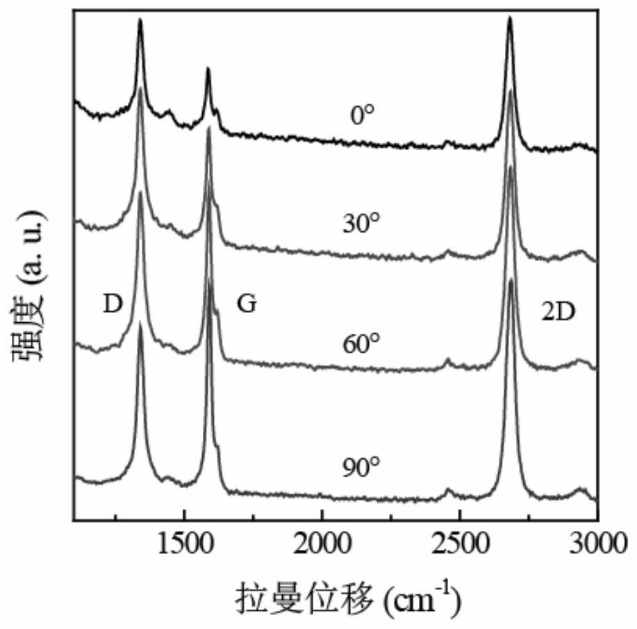
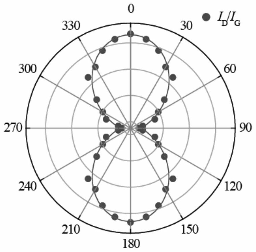
[0026] Hydrogen plasma etching is performed on the patterned graphene to obtain graphene strips with neat edges (also referred to as graphene nano-strips).
[0027] In some specific embodiments, the preparation method further includes: before performing photolithography patterning, firstly transferring the graphene to the substrate.
[0028] Specifically, the preparation method includes: patterning by ordinary lithography or electron beam lithography, migrating graphene to the substrate, and then exposing the required pattern by photolithography or electron beam lithography, and the pattern size can be in the nanometer The scale can also be on the micrometer scale. That ...
Embodiment 1
[0057] The method for preparing neat edge graphene strips in the present embodiment comprises the following steps:
[0058] (1) The substrate material was thermally oxidized to grow a silicon wafer of 300 nm silicon dioxide, and the graphene was migrated after cleaning the substrate.
[0059] (2) Ordinary lithography or electron beam lithography, apply glue to the graphene-migrated sample on the substrate, and then use lithography or electron beam lithography to expose the desired pattern, and the pattern size can be in the nanoscale or in the micron scale.
[0060] (3) Growth of metal film: Magnetron sputtering was used to grow zinc with a thickness of 20 nm on the sample after photolithography and development.
[0061] (4) Hydrogen plasma etching: at room temperature, pure hydrogen plasma is used, the power is set to 50W, the flow rate of 100SCCM is adopted, the air pressure is 600Pa, and the etching time is 5 minutes. During the etching process, a vacuum pump is used to k...
Embodiment 2
[0063] The method for preparing neat edge graphene strips in the present embodiment comprises the following steps:
[0064] (1) Silicon wafers with 100 nm silicon dioxide were grown by thermal oxidation of substrate material, and graphene was migrated after cleaning the substrate.
[0065] (2) Ordinary lithography or electron beam lithography, apply glue to the graphene-migrated sample on the substrate, and then use lithography or electron beam lithography to expose the desired pattern, and the pattern size can be in the nanoscale or in the micron scale.
[0066] (3) Growth of metal film: Magnesium with a thickness of 1 nm was grown on the photolithographic and developed sample using magnetron sputtering.
[0067] (4) Hydrogen plasma etching: at room temperature, pure hydrogen plasma is used, the power is set to 100W, the flow rate of 10SCCM is adopted, the air pressure is 60Pa, and the etching time is 60 minutes. During the etching process, a vacuum pump is used to keep the...
PUM
| Property | Measurement | Unit |
|---|---|---|
| electrical resistance | aaaaa | aaaaa |
| thickness | aaaaa | aaaaa |
| width | aaaaa | aaaaa |
Abstract
Description
Claims
Application Information


