Gene sequencing chip and gene sequencing method

A gene sequencing and chip technology, applied in the fields of biochemical equipment and methods, microbial determination/inspection, biochemical instruments, etc., can solve the problem of fluorescence detection technology, expensive labeling reagents or autofluorescence reaction system, sequence analysis continuity and simultaneous monitoring and reflection Insufficient quantity, cost reduction and other problems, to achieve the effect of improving integration and stability, reducing excitation area and reducing cost

Active Publication Date: 2019-06-04
INST OF SEMICONDUCTORS - CHINESE ACAD OF SCI
View PDF7 Cites 7 Cited by
  • Summary
  • Abstract
  • Description
  • Claims
  • Application Information

AI Technical Summary

Problems solved by technology

[0003] Since the current DNA sequencing technologies are all indirect sequencing, that is, based on the observation of labeled fluorescence or autofluorescence during the enzymatic biochemical reaction of nucleic acids, such technologies are limited by the fluorescence attenuation caused by "enzyme fatigue" and the optical Due to factors such as the size of the detection device, the continuity of sequence analysis and the number of simultaneous monitoring reactions are insufficient, resulting in short read length or low throughput
At the same time, fluorescence detection technology requires expensive labeling reagents or autofluorescence reaction systems, making it difficult to further reduce costs on the basis that the throughput level has almost reached the limit

Method used


Image

  • Gene sequencing chip and gene sequencing method
  • Gene sequencing chip and gene sequencing method
  • Gene sequencing chip and gene sequencing method

Examples


Embodiment 1

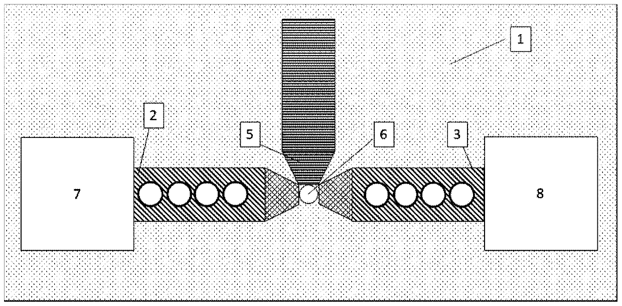
[0046] figure 1 A schematic structural diagram of a gene sequencing chip based on tip-enhanced Raman effect in Example 1 of the present invention is shown. Such as figure 1 As shown, the chip includes:

[0047] A substrate 1 , a first optical waveguide 2 , a second optical waveguide 3 , a metal tip 5 , a nanohole 6 , a light source coupling module 7 , and a first signal acquisition module 8 . The first optical waveguide 2 , the second optical waveguide 3 , the metal needle tip 5 , the nanohole 6 , the light source coupling module 7 , and the first signal acquisition module 8 are all formed on the substrate 1 .

[0048] The substrate 1 is a silicon substrate, the first optical waveguide 2, the second optical waveguide 3 and the metal needle point 5 are relatively distributed on the silicon substrate in a T shape, and the nanohole 6 is arranged on the first optical waveguide 2 and the second optical waveguide 3 The area in contact with the metal needle tip 5 runs through the ...

Embodiment 2

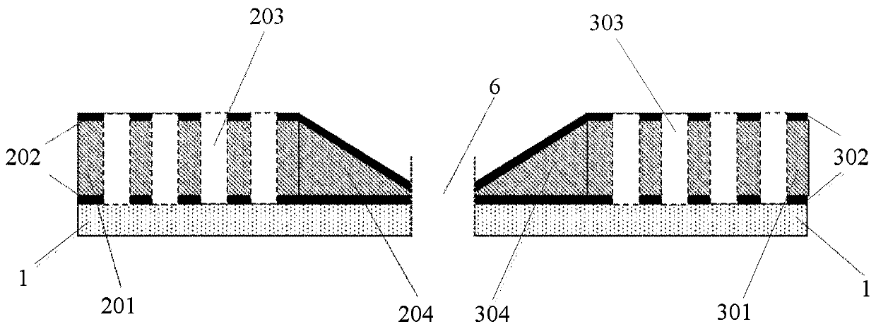
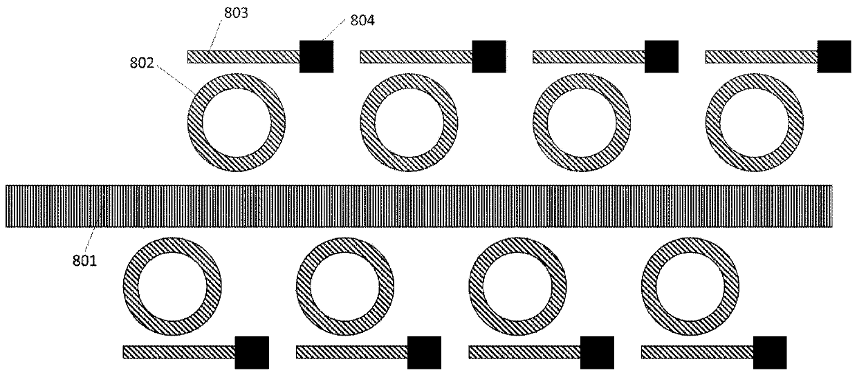
[0053] On the basis of the gene sequencing chip based on the tip-enhanced Raman effect described in Example 1, this example adds a second Raman signal acquisition method, such as Figure 4 As shown, the gene sequencing chip also includes a third optical waveguide 4 and a second collector 9, which are formed on the substrate 1, and the third optical waveguide 4 is opposite to the T-shaped first optical waveguide 2 and the second optical waveguide. 3 and the metal needle point 5 form a cross-shaped structure, the nanohole 6 is placed in the middle of the cross, the third optical waveguide 4 has a three-dimensional gradient structure, and one end is opposite to the metal needle point 5, and the second collector 9 is located on the third optical waveguide 4 and has a three-dimensional gradient structure. One end of the structure is opposite to the other end, the third optical waveguide 4 is a MIM structure, and the metal material in the MIM structure is a metal with a strong surfac...

Embodiment 3

[0056] This embodiment proposes a gene sequencing method based on a gene sequencing chip, such as Figure 5 As shown, the methods include:

[0057] S1, the optical field of the optical signal generated by the light source coupler 7 passes through the first optical waveguide 2 and the second optical waveguide 3 for compression enhancement and resonance enhancement to form excitation light.

[0058] Specifically, the optical signal sent by the light source coupler 7 is reflected back and forth by at least one Bragg periodic structure 203 (303) on the first optical waveguide 2 and the second optical waveguide 3, realizing resonance enhancement, and passing through the three-dimensional tapered structure 204 (304) The optical signal light field is further compressed and enhanced to form excitation light.

[0059] S2, controlling the base chain of the gene to be tested to pass through the nanopore 6 in the form of a single strand;

[0060] Because the size of the nanopore 6 is la...


PUM

PropertyMeasurementUnit
sizeaaaaaaaaaa

Abstract

The invention discloses a gene sequencing chip and a gene sequencing method. The gene sequencing chip comprises a substrate (1), a first optical waveguide (2), a second optical waveguide (3), a metalneedle tip (5), nano-pores (6); the first optical waveguide (2), the second optical waveguide (3) and the metal needle tip (5) are all formed, in T-shaped relative distribution, on the substrate (1);the first optical waveguide (2) and the second optical waveguide (3) are oppositely positioned; the nano-pores (6) are arranged in contact areas of the first optical waveguide (2), the second opticalwaveguide (3) and the metal needle tip (5), and penetrate through the substrate (1); one ends of the first optical waveguide (2) and the second optical waveguide (3) are both three-dimensional taperedstructures; the first optical waveguide (2) and the second optical waveguide (3) are opposite to each other by the ends with the three-dimensional tapered structures; a light source coupler (7) is arranged, on the other end opposite to the end with the three-dimensional tapered structure, on the first optical waveguide (2); and a first signal collector (8) is arranged, on the other end opposite to the end with the three-dimensional tapered structure, on the second optical waveguide (3). The gene sequencing chip and the gene sequencing method improve detection efficiency of base monomers, thereby reducing cost with integration level and stability of the chip system improved; moreover, data volume is reduced so as to have collection rate improved.

Description

technical field [0001] The invention relates to the field of gene sequencing, in particular to a gene sequencing chip and method. Background technique [0002] Nucleotide sequencing technology is one of the key and basic technologies in genomics and even life science research. It is also the main means of obtaining basic biological information data and the driving force behind the development of biological computing and bioinformatics. Since the birth of Sanger sequencing method, sequencing technology has greatly promoted the development of life science and medicine. In the past 10 years, the successful application of high-throughput second-generation DNA sequencing technology has once again promoted the rapid development of the field of medical and life sciences, and has given birth to the emergence of "precision medicine". However, all second-generation DNA sequencing technologies utilize biochemical reactions of DNA polymerase or ligase to determine DNA sequencing indire...

Claims


Application Information

Patent Timeline
Patent Type & Authority Applications(China)
IPC IPC(8): C12M1/34C12M1/00C12Q1/6874
Inventor 胡诗铭节俊尧刘文文魏清泉任鲁风俞育德
Owner INST OF SEMICONDUCTORS - CHINESE ACAD OF SCI
Why Eureka
Try Eureka