Magnetoresistive sensor structure and manufacturing method thereof

A magnetoresistive sensor and manufacturing method technology, applied in the fields of magnetic field controlled resistors, manufacturing/processing of electromagnetic devices, components of electromagnetic equipment, etc., can solve problems such as difficulty, high cost, and complicated manufacturing process of TMR sensors, Achieve good protection, improve yield, and avoid the effect of removing the residual metal film

CN109888088AActive Publication Date: 2019-06-14XI AN JIAOTONG UNIV
7 Cites 6 Cited by

Patent Information

Authority / Receiving Office
CN · China
Current Assignee / Owner
Publication Date
2019-06-14

Smart Images

  • Figure 1
    Figure 1
  • Figure 2
    Figure 2
Patent Text Reader

Abstract

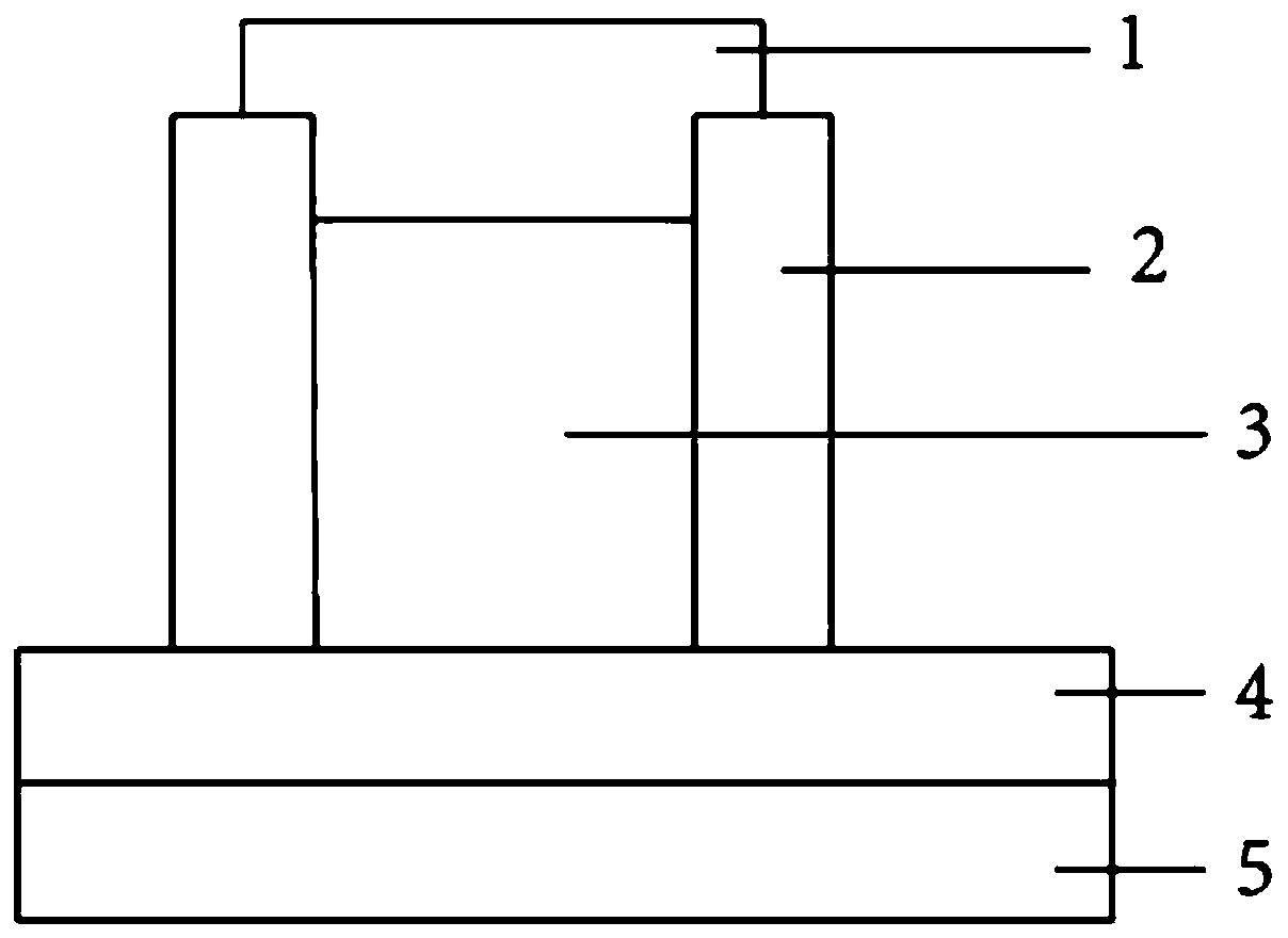
The invention discloses a magnetoresistive sensor structure and a manufacturing method thereof. The magnetoresistive sensor structure comprises a substrate, a buffer layer, a phase change structure, insulation layers and a conductive material electrode, wherein the buffer layer is arranged on the upper surface of the substrate; the phase change structure and the insulation layers are arranged on the buffer layer; the insulation layers are arranged on two sides of the phase change structure; the insulation layers are higher than the phase change structure; the conductive material electrode is arranged between tops of the two insulation layers; and the phase change structure comprises a ferromagnetic layer, a phase change material and a non-magnetic layer. The phase change material is used as a non-magnetic isolation layer, and the insulation phase change material can be converted into a conductive material under the function of current at room temperature, so that the magnetoresistive sensor can be controllably overturned between two effects such as GMR and TMR, thereby realizing the dynamic control of a linear measurement range of the magnetoresistive sensor.
Need to check novelty before this filing date? Find Prior Art

Description

technical field

[0001] The invention belongs to the technical field of magnetoresistive sensors, and in particular relates to a magnetoresistive sensor structure and a manufacturing method thereof. Background technique

[0002] Magnetoresistance sensors include AMR (Anisotropy Magnetoresistance, anisotropic magnetoresistance) sensors, GMR (Giant Magnetoresistance, giant magnetoresistance) sensors and TMR (Tunnel Magnetoresistance, tunnel magnetoresistance) sensors, with high integration, low offset, and high sensitivity , good temperature performance and other advantages, it has been widely used in automotive electronics, precision measurement and other fields. The magnetoresistance of the magnetoresistive sensor changes with the magnitude and direction of the applied magnetic field, so it is used to detect the magnetic field. Its sensitivity is better than that of the Hall sensor, and it has better temperature stability and lower power consumption. In addition, the process...

Examples

Embodiment 1

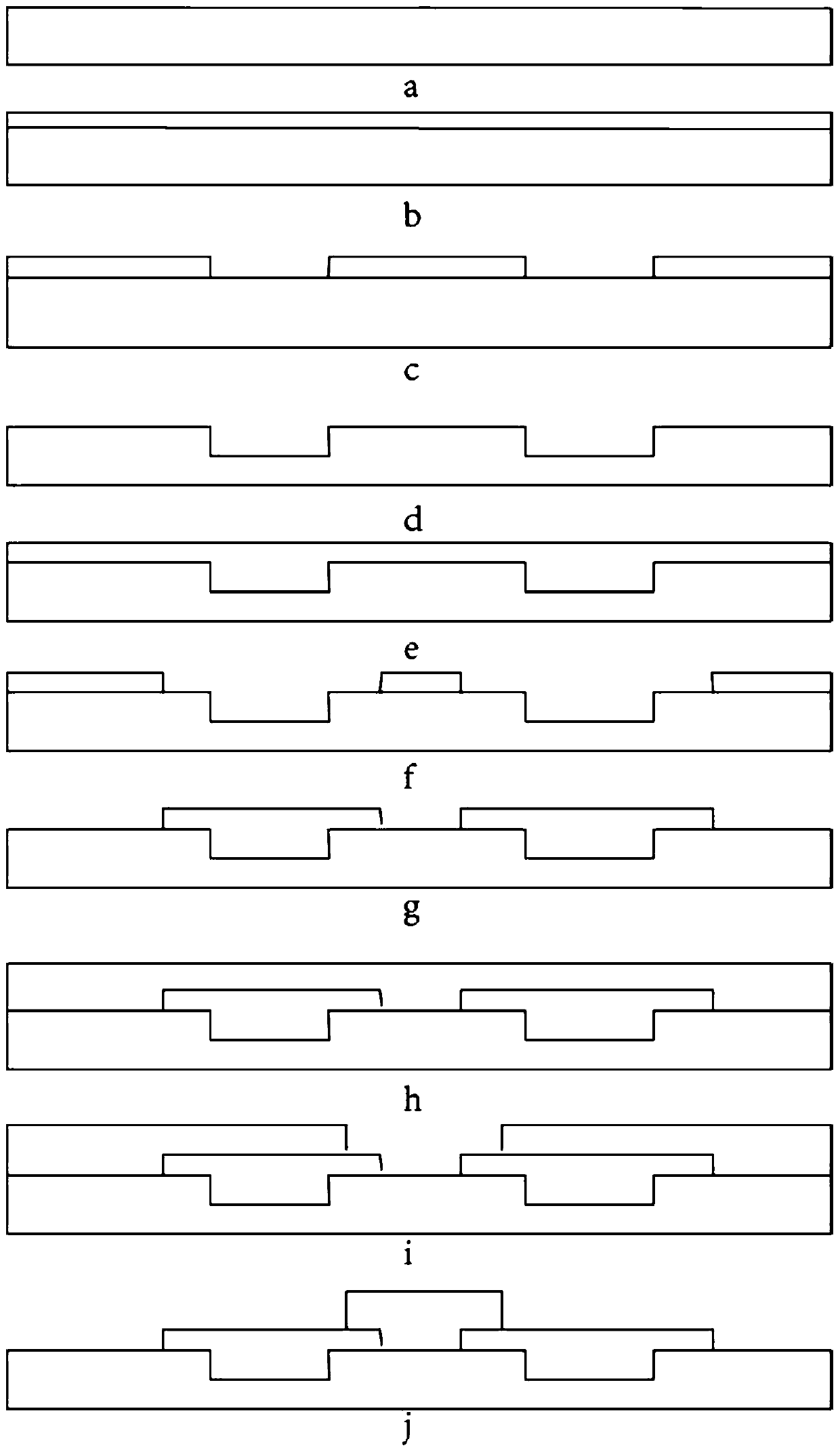
[0065] Step 1: Provide a Si substrate, use acetone, alcohol, and deionized water to ultrasonically clean it for 5 minutes, then blow dry it with N2, and keep it in an oven at 115°C for 20 minutes.

[0066] Step 2, the model of the photoresist used in the present invention is APR-3510P. After the photoresist is dropped on the Si substrate, the photoresist is first rotated at a rate of 600 rpm for 10s so that the photoresist covers the Si sheet, and then 4000 rpm Rotate at a rate of 40s to make the photoresist thickness uniform.

[0067] Step 3, put the Si substrate spin-coated with photoresist into an oven, and heat it at 115° C. for 20 minutes, so that the photoresist is completely cured.

[0068] Step 4, exposing the first photoresist layer to ultraviolet light through the mask plate of the first predefined pattern.

[0069] Step 5, develop, remove excess photoresist, and leave a first predefined pattern on the Si substrate.

[0070] Step 6, using magnetron sputtering thin ...