Silicon carbide MOSFET (Metal-Oxide -Semiconductor Field Effect Transistor) device capable of integrating with high-speed reverse free-wheeling diode

A reverse freewheeling and diode technology, applied in electric solid devices, semiconductor devices, electrical components, etc., can solve the problems of low doping concentration, high conduction voltage drop, high conduction voltage drop, reverse recovery time, etc. , to achieve the effects of high channel mobility, low on-resistance, improved integration and application cost

Active Publication Date: 2019-06-18
UNIV OF ELECTRONICS SCI & TECH OF CHINA
View PDF8 Cites 12 Cited by
  • Summary
  • Abstract
  • Description
  • Claims
  • Application Information

AI Technical Summary

Problems solved by technology

The traditional method is to connect a FWD in parallel outside the power device, or to package the FWD and the power device together; for silicon carbide power devices, due to the high conduction voltage drop of conventional silicon carbide PN junction diodes, at the same time for power As far as the device is concerned, it has a thicker layer of drift region with a lower doping concentration. Therefore, the reverse freewheeling PIN diode made by the body region of the power device itself has a higher turn-on voltage drop, reverse recovery time and loss

Method used


Image

  • Silicon carbide MOSFET (Metal-Oxide -Semiconductor Field Effect Transistor) device capable of integrating with high-speed reverse free-wheeling diode
  • Silicon carbide MOSFET (Metal-Oxide -Semiconductor Field Effect Transistor) device capable of integrating with high-speed reverse free-wheeling diode
  • Silicon carbide MOSFET (Metal-Oxide -Semiconductor Field Effect Transistor) device capable of integrating with high-speed reverse free-wheeling diode

Examples


Embodiment 1

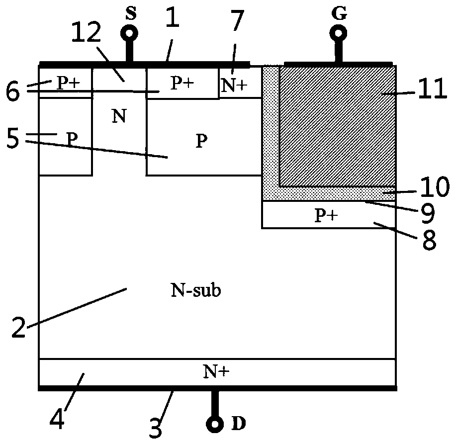
[0039] This embodiment provides a new type of insulated gate power device integrating an inversion layer channel of a high-speed reverse freewheeling diode, and its structure is as follows figure 1 As shown, it includes a metallized source 1, an N-type drift region 2, and a metallized drain 3 stacked sequentially from top to bottom, wherein:

[0040] The lower surface of the N-type drift region 2 is a back structure, and the back structure includes: an N-type drain region 4, and the N-type drain region 4 forms an ohmic contact with the upper surface of the metallized drain 3;

[0041] The upper surface of the N-type drift region 2 is a front structure, and the front structure includes: a first P-type region 5, a P-type source region 6, an N-type source region 7, a second P-type region 8, a first N-type region 12, trench 9 and oxide layer 10 and gate 11 in the trench; the trench 9 is opened on one side of the upper surface of the N-type drift region 2, and the interior of the t...

Embodiment 2

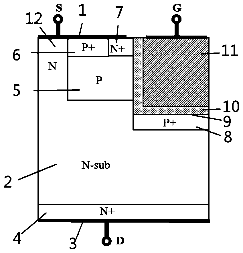
[0048] This embodiment provides a new type of accumulation channel insulated gate power device integrating a high-speed reverse freewheeling diode, and its structure is as follows image 3 As shown, the difference between it and Embodiment 1 is that the device also includes a second N-type region 13, and the upper and lower sides of the second N-type region 13 are respectively in phase with the N-type source region 7 and the N-type drift region 2. Contacts, left and right are in contact with the first P-type region 5 and the oxide layer 10 respectively.

[0049] The working principle of this embodiment is as follows:

[0050] In this embodiment, a new type of insulated gate power device integrating the inversion layer channel of the high-speed reverse freewheeling diode, the electrode connection mode during forward conduction is: the metallized drain (D) is connected to a high potential, and the metallized drain (D) is connected to a high potential. The source (S) is connecte...

Embodiment 3

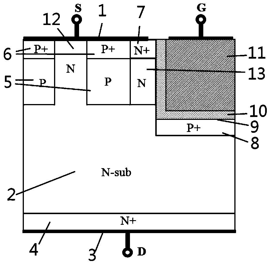
[0055] This embodiment provides a new type of insulated gate power device integrating an inversion layer channel of a high-speed reverse freewheeling diode, and its structure is as follows Figure 5 As shown, the difference between it and Embodiment 1 is that the device further includes a third P-type region 14 , and the third P-type region 14 is disposed below the second P-type region 8 .

[0056] The working principle of the device in this embodiment is the same as that in Embodiment 1, wherein, when the device is blocked, the first P-type region 5, the second P-type region 8, and the third P-type region 14 are in common with the PN junction of the N-type drift region 2 Withstanding voltage, the introduction of the third P-type region 14 can help to increase the withstand voltage of the device, and at the same time, under the condition that the blocking withstand voltage remains unchanged, the on-resistance of the forward conduction can be reduced.


PUM


Abstract

The invention belongs to the technical field of semiconductor power devices, and relates to a silicon carbide semiconductor device, in particular to a silicon carbide MOSFET (Metal-Oxide-SemiconductorField Effect Transistor) device capable of integrating with a high-speed reverse free-wheeling diode for realizing the integration of the silicon carbide semiconductor device and the reverse free-wheeling diode. Compared with the original body diode of silicon carbide MOSFET, the integrated Schottky barrier FWD (Free-Wheeling Diode) can realize low diode conduction pressure drop and reduce reverse recovery time and loss. By use of the device, the application cost of the silicon carbide power semiconductor device and the number of peripheral devices when the device is applied can be favorablylowered, and therefore, the device has a large application value.

Description

technical field [0001] The invention belongs to the technical field of semiconductor power devices, and relates to a silicon carbide power semiconductor device, in particular to a silicon carbide MOSFET device integrating a high-speed reverse freewheeling diode. Background technique [0002] Compared with silicon materials, silicon carbide materials have excellent characteristics such as larger band gap, higher carrier saturation rate and larger thermal conductivity, so the performance of power electronic devices made of silicon carbide materials far exceeds that of silicon Materials; Power devices made of silicon carbide materials have lower conduction losses, switching losses and better voltage blocking capabilities, so they have broad application prospects. [0003] Usually, most power devices are used in switching circuits with inductive loads, which requires an anti-parallel free-wheeling diode (FWD) for the power devices. The traditional method is to connect a FWD in ...

Claims


Application Information

Patent Timeline
Patent Type & Authority Applications(China)
IPC IPC(8): H01L27/07H01L29/06H01L29/10H01L29/16
Inventor 孔谋夫
Owner UNIV OF ELECTRONICS SCI & TECH OF CHINA
Why Eureka
Try Eureka