Field-effect transistor manufacturing method and field-effect transistor

A manufacturing method and field effect tube technology, which is applied in semiconductor/solid-state device manufacturing, electrical components, circuits, etc., can solve problems such as high cost and complicated process

Pending Publication Date: 2019-06-18
SHANGHAI IND U TECH RES INST
View PDF4 Cites 5 Cited by
  • Summary
  • Abstract
  • Description
  • Claims
  • Application Information

AI Technical Summary

Problems solved by technology

So far, the reported processes for fabricating SiGe nanowires are complicated, and the Damaccus pseudo-gate proc

Method used


Image

  • Field-effect transistor manufacturing method and field-effect transistor
  • Field-effect transistor manufacturing method and field-effect transistor
  • Field-effect transistor manufacturing method and field-effect transistor

Examples


Embodiment Construction

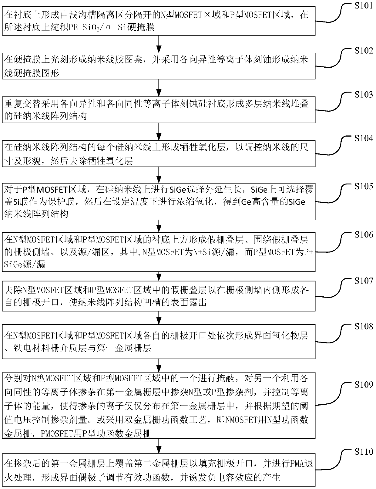
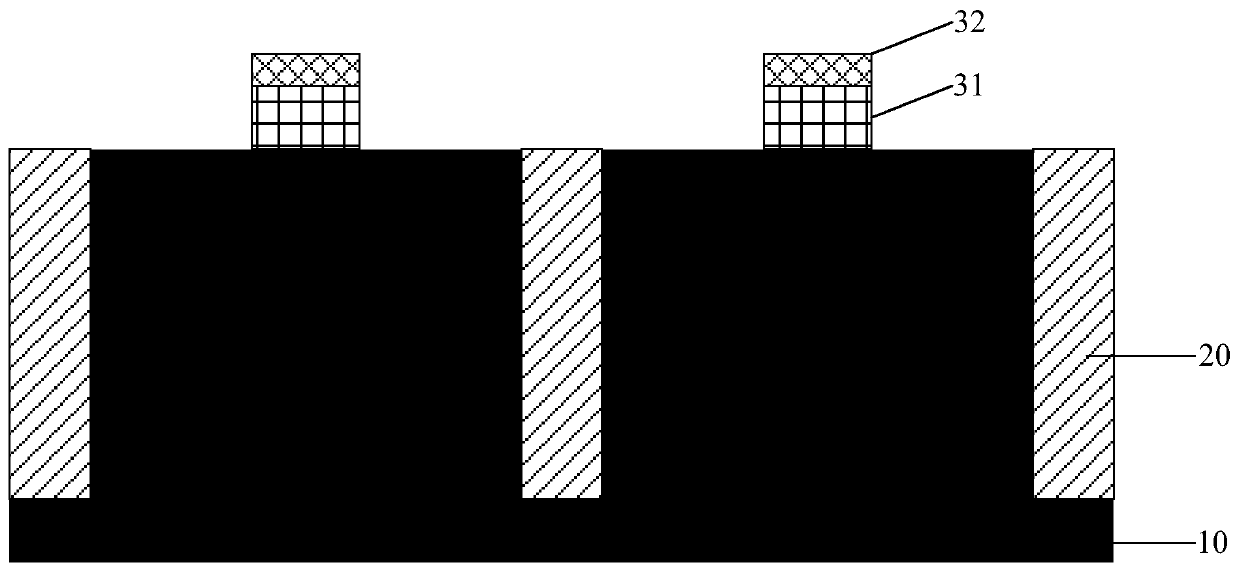
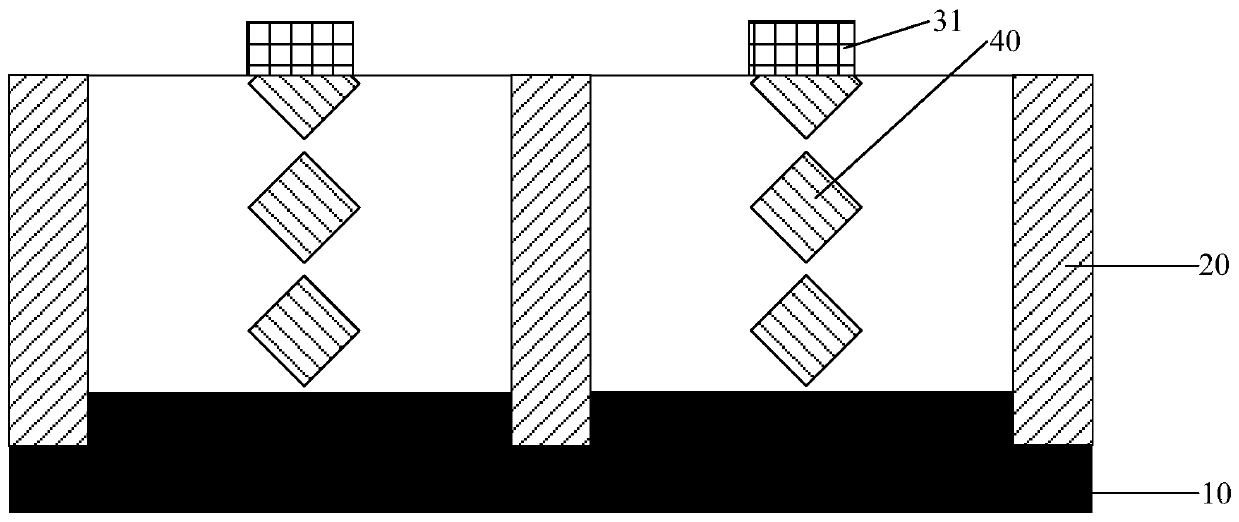
[0080]The present disclosure is to provide a ferroelectric material negative capacitance nanowire array ring-gate complementary field effect transistor structure and a manufacturing method thereof. The ferroelectric material negative capacitance nanowire array ring-gate CMOSFET structure has an N-type MOSFET region and a P-type MOSFET at the same time. area, not only retains the good electron mobility of the Si nanowire gate NMOSFET, but also improves the hole mobility of the SiGe nanowire gate PMOSFET. Moreover, because the nanowire ring-gate structure greatly improves the gate control ability, it suppresses the short-channel effect extremely well. In particular, the nanowire array ring-gate CMOSFET structure of the present disclosure integrates the ferroelectric negative capacitance effect, which effectively increases the surface potential of the device channel, making it greater than the external gate voltage, which realizes the voltage amplification effect and breaks throug...


PUM

PropertyMeasurementUnit
Thicknessaaaaaaaaaa
Thicknessaaaaaaaaaa
Thicknessaaaaaaaaaa

Abstract

The invention discloses a field-effect transistor manufacturing method and a field-effect transistor. The method comprises the following steps of forming an N-type MOSFET region and a P-type MOSFET region on a substrate; forming a hard mask pattern on the MOSFET region; forming a silicon nanowire array structure; forming a sacrificial oxidization layer on the multi-layer stacked silicon nanowires,and then removing the sacrificial oxidization layer; carrying out selective SiGe epitaxy and concentration oxidation on the multi-layer stacked silicon nanowires of the P-type MOSFET region, and removing the oxidization layer; and sequentially forming an interface oxide layer, a ferroelectric material gate dielectric laminated layer and a metal gate laminated layer on the nanowire array structure. According to the field-effect transistor, the gate-control capability is greatly enhanced due to the ring gate structure; due to the PMOSFET SiGe nanowires and the SiGe source/drain, the hole mobility is greatly improved; and especially due to the fact that the ferroelectric negative capacitance effect is integrated, the potential on the surface of a channel of the device is amplified, so that the nanowire device has a super-steep sub-threshold slope and an improved on/off current ratio.

Description

technical field [0001] The disclosure belongs to the technical field of semiconductors, and relates to a manufacturing method of a field effect tube and the field effect tube. Background technique [0002] As the feature size of integrated circuits becomes smaller and smaller, planar CMOS devices have encountered serious challenges, and various new device structures have emerged. The gate structure of devices has evolved from traditional planar single gates to double gates, triple gates, and completely wrapped channel. The gate-enclosed structure, gate control ability and ability to control short channel effects are continuously enhanced, and MOSFETs with nanowire gate-enclosed structure (GAA) with quasi-ballistic transmission characteristics are widely used due to their strong gate control ability and size reduction ability. Attach great importance to it and become a strong competitor in the technology generation of 3nm and below. However, when the device size enters the t...

Claims


Application Information

Patent Timeline
IPC IPC(8): H01L29/06H01L21/336H01L29/78
Inventor 徐秋霞胡正明陈凯
Owner SHANGHAI IND U TECH RES INST
Why Eureka
Try Eureka