Light-emitting diode epitaxial wafer and preparation method thereof, light-emitting diode

A technology of light-emitting diodes and epitaxial wafers, applied in the field of epitaxy, can solve the problems of poor crystal quality of P-type AlGaN layer, entry of P-type AlGaN layer, unfavorable electrons, etc., to improve crystal quality, increase hole concentration, and improve doping uniformity sexual effect

Active Publication Date: 2020-12-01
HC SEMITEK ZHEJIANG CO LTD
View PDF4 Cites 0 Cited by
  • Summary
  • Abstract
  • Description
  • Claims
  • Application Information

AI Technical Summary

Problems solved by technology

[0004] However, the crystal quality of the P-type AlGaN layer in the current epitaxial wafer structure is usually poor.

Method used


Image

  • Light-emitting diode epitaxial wafer and preparation method thereof, light-emitting diode
  • Light-emitting diode epitaxial wafer and preparation method thereof, light-emitting diode
  • Light-emitting diode epitaxial wafer and preparation method thereof, light-emitting diode

Examples


Embodiment Construction

[0029] In order to make the object, technical solution and advantages of the present invention clearer, the implementation manner of the present invention will be further described in detail below in conjunction with the accompanying drawings.

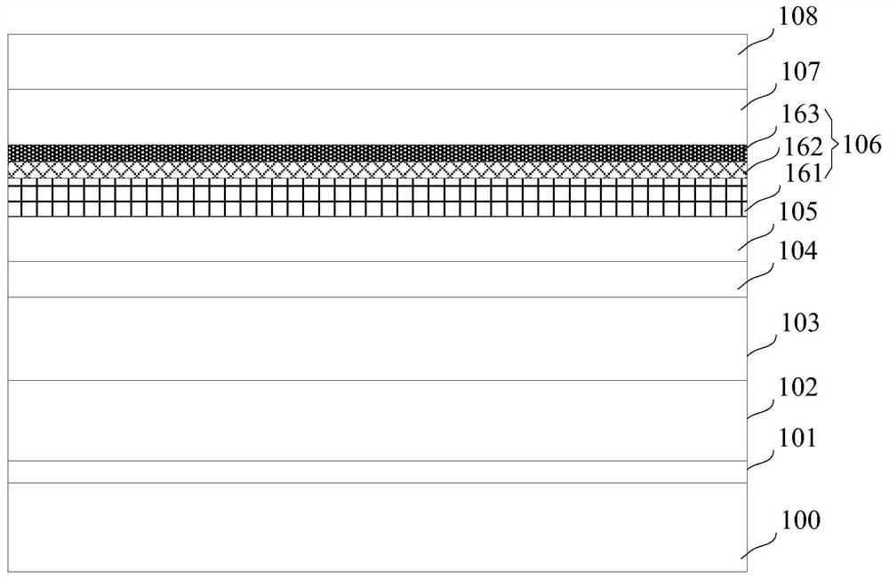
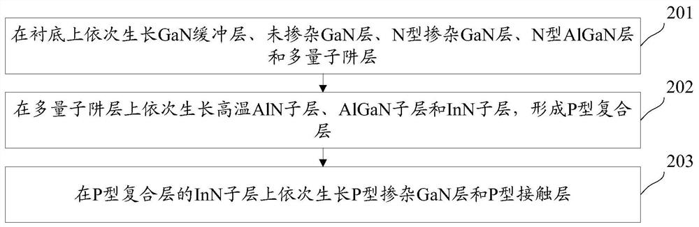
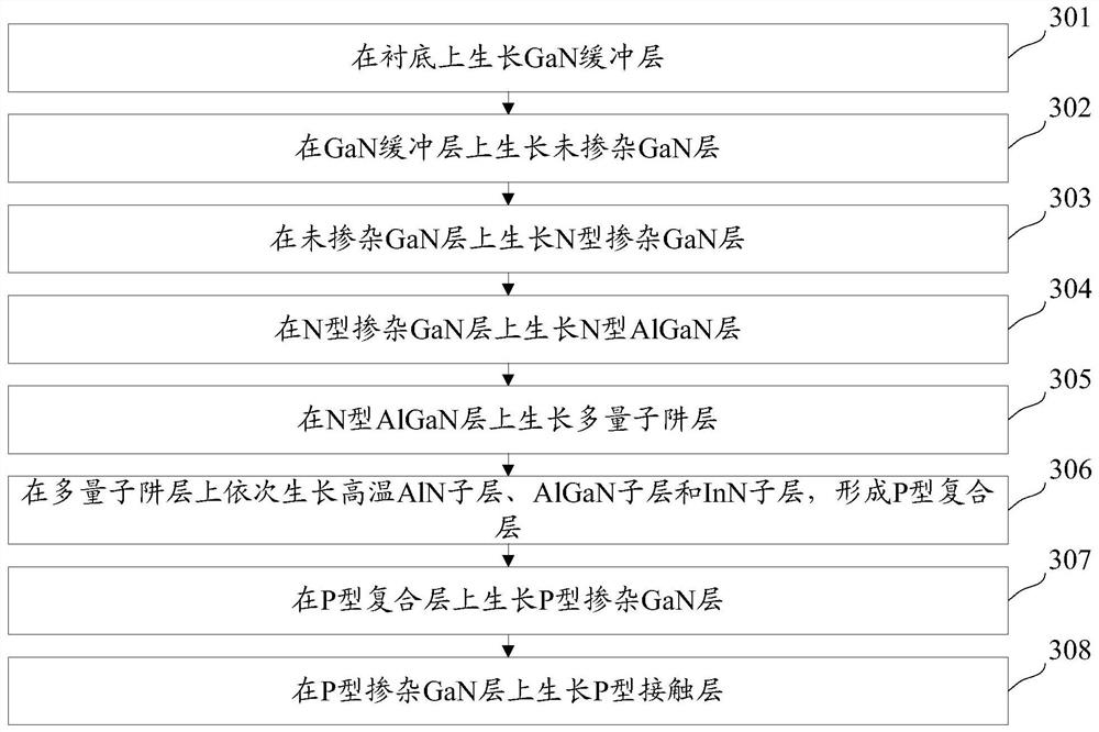
[0030] figure 1 It is a schematic structural diagram of a light emitting diode epitaxial wafer provided by an embodiment of the present invention. see figure 1 , the light-emitting diode epitaxial wafer may include: a substrate 100, and a GaN buffer layer 101, an undoped GaN layer 102, an N-type doped GaN layer 103, an N-type AlGaN layer 104, and a multi-quantum layer stacked sequentially on the substrate 100. Well layer 105 , P-type composite layer 106 , P-type doped GaN layer 107 and P-type contact layer 108 .

[0031] Wherein, the P-type composite layer 106 may include: a high-temperature AlN sublayer 161 located on the multi-quantum well layer, an AlGaN sub-layer 162 located on the high-temperature AlN sub-layer 161, and an In-co...


PUM

PropertyMeasurementUnit
thicknessaaaaaaaaaa
thicknessaaaaaaaaaa
thicknessaaaaaaaaaa

Abstract

The invention discloses a light emitting diode, and an epitaxial wafer and a preparation method thereof, and belongs to the technical field of epitaxy. The epitaxial wafer of the light emitting diodecomprises: a substrate, and a gallium nitride buffer layer, an undoped gallium nitride layer, an N-type doped gallium nitride layer, an N-type aluminum gallium nitride layer, a multi-quantum well layer, a P-type composite layer, a P-type doped gallium nitride layer and a P-type contact layer, which are laminated on the substrate in sequence; the P-type composite layer comprises: a high-temperaturealuminum nitride sub-layer located on the multi-quantum well layer, an aluminum gallium nitride sub-layer located on the high-temperature aluminum nitride sub-layer, and an indium-containing nitridesub-layer located on the aluminum gallium nitride sub-layer, and the P-type doped gallium nitride layer is located on the indium-containing nitride sub-layer. By means of the P-type composite layer comprising three sub-layers, the electron blocking effect is improved on one hand, and the smooth pass of holes is ensured on the other hand.

Description

technical field [0001] The invention relates to the field of epitaxy technology, in particular to a light-emitting diode epitaxial wafer, a preparation method thereof, and a light-emitting diode. Background technique [0002] Currently, Gallium Nitride (GaN)-based Light Emitting Diodes (Light Emitting Diodes, LEDs) are receiving more and more attention and research. The epitaxial wafer is the core part of the GaN-based LED. The structure of the epitaxial wafer includes: substrate, GaN buffer layer, undoped GaN layer, N-type doped GaN layer, N-type aluminum gallium nitride (AlGaN) layer, multiple quantum wells ( Multiple Quantum Well, MQW) layer, P-type AlGaN layer, P-type doped GaN layer and P-type contact layer. [0003] When a current flows, electrons in the N-type doped GaN layer and holes in the P-type doped GaN layer enter the MQW layer, and recombine and emit light in the MQW layer. However, when electrons and holes recombine in other layers outside the MQW layer, th...

Claims


Application Information

Patent Timeline
Patent Type & Authority Patents(China)
IPC IPC(8): H01L33/06H01L33/12H01L33/14H01L33/32H01L33/00
Inventor 曹阳乔楠郭炳磊吕蒙普胡加辉李鹏
Owner HC SEMITEK ZHEJIANG CO LTD
Why Eureka
Try Eureka