A kind of three-layer nanoporous film and its preparation method and application

A nanoporous film and nanofilm technology, applied in the field of biochemical detection materials, can solve the problems of inaccurate detection results and low spatial resolution of DNA sequencing of three-layer nanoporous film, and achieve good adhesion, stable thin layer quality, Uniform and controllable thickness

Active Publication Date: 2021-03-30
GUANGDONG UNIV OF TECH
View PDF6 Cites 0 Cited by
  • Summary
  • Abstract
  • Description
  • Claims
  • Application Information

AI Technical Summary

Problems solved by technology

[0004] The technical problem to be solved by the present invention is to overcome the defects and deficiencies of the existing three-layer nanoporous film DNA sequencing that the spatial resolution is not high and the detection results are not accurate enough, and provide a three-layer nanoporous film

Method used


Image

  • A kind of three-layer nanoporous film and its preparation method and application
  • A kind of three-layer nanoporous film and its preparation method and application
  • A kind of three-layer nanoporous film and its preparation method and application

Examples


Embodiment 1

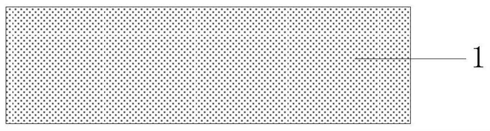
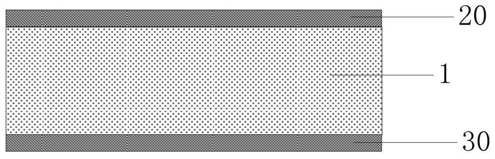
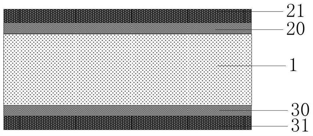
[0046] A preparation method of a three-layer nanoporous film, such as Figure 1~4 , shown in 6-8, 10, including the following steps:

[0047] S1. On the surface of both sides of the doped single crystal silicon substrate 1, adopt low-pressure chemical vapor deposition (LP-CVD) to deposit Si 3 N 4 layers (20 and 30), in Si 3 N 4 Layer surface continues to SiO 2 layers (21 and 31), forming Si 3 N 4 / SiO 2 double-layer nanostructure, where Si 3 N 4 layer thickness of 30nm, SiO 2 The thickness of the layer is 40 nm;

[0048] S2. Using atomic layer deposition of Si on one side of the substrate 3 N 4 / SiO 2 Deposition of Si on bilayer nanofilms 3 N 4 Layer 22, Si 3 N 4 layer thickness 5nm, forming Si 3 N 4 / SiO 2 / Si 3 N 4 Three-layer nanostructure;

[0049] S3. Si on the above substrate 3 N 4 / SiO 2 One side of the bilayer nanostructure etches Si by reactive ion etching 3 N 4 / SiO 2 The layer forms the matrix release window 4, and the size range of the ...

Embodiment 2

[0054] A preparation method of a three-layer nanoporous film, comprising the steps of:

[0055] S1. Deposit Si on both sides of the doped polysilicon substrate by low-pressure chemical vapor deposition (LP-CVD) 3 N 4 layer, in Si 3 N 4 Layer surface continues to SiO 2 layer, forming Si 3 N 4 / SiO 2 double-layer nanostructure, where Si 3 N 4 layer thickness of 100nm, SiO 2 The thickness of the layer is 100nm;

[0056] S2. Using atomic layer deposition of Si on one side of the substrate 3 N 4 / SiO 2 Deposition of Si on bilayer nanofilms 3 N 4 layer, Si 3 N 4 layer thickness 5nm, forming Si 3 N 4 / SiO 2 / Si 3 N 4 Three-layer nanostructure;

[0057] S3. Si on the above substrate 3 N 4 / SiO 2 One side of the bilayer nanostructure etches Si by reactive ion etching 3 N 4 / SiO 2 The layer forms a matrix release window with a size range of 800 μm × 800 μm;

[0058] S4. Use an alkaline solution to etch the substrate from the substrate release window to obtai...

Embodiment 3

[0062] A preparation method of a three-layer nanoporous film, comprising the steps of:

[0063] S1. adopt low-pressure chemical vapor deposition (LP-CVD) to deposit Si on the surface of both sides of the germanium substrate 1 after doping 3 N 4 layer, in Si 3 N 4 Layer surface continues to SiO 2 layer, forming Si 3 N 4 / SiO 2 double-layer nanostructure, where Si 3 N 4 layer thickness of 200nm, SiO 2 The thickness of the layer is 200nm;

[0064] S2. Using atomic layer deposition of Si on one side of the substrate 3 N 4 / SiO 2 Deposition of Si on bilayer nanofilms 3 N 4 layer, Si 3 N 4 layer thickness 5nm, forming Si 3 N 4 / SiO 2 / Si 3 N 4 Three-layer nanostructure;

[0065] S3. Si on the above substrate 3 N 4 / SiO 2 One side of the bilayer nanostructure etches Si by reactive ion etching 3 N 4 / SiO 2 The layer forms a matrix release window with a size range of 800 μm × 800 μm;

[0066] S4. Use an alkaline solution to etch the substrate from the substra...


PUM

PropertyMeasurementUnit
thicknessaaaaaaaaaa
pore sizeaaaaaaaaaa
thicknessaaaaaaaaaa

Abstract

The invention discloses a three-layer nanopore thin film and a preparation method and application thereof. The preparation method comprises the following steps that a base plate is provided, two-layerSi3N4 / SiO2 nano thin films deposit on the surfaces of the two sides of the base body, a layer of Si3N4 thin film deposits on the top SiO2 thin film layer, the thin film on one side of the base boy isetched to form a base body releasing window, the base plate is etched so that the three-layer nano thin film can be obtained, reactive ion etching is adopted to etch the Si3N4 thin film on the releasing window of the base body to achieve thinning, a suspended three-layer nano thin film structure is obtained, and helium ion beams are used for carrying out etching so that a three-layer nano throughhole can be obtained. According to the preparation method for the three-layer nanopore thin film, an Si3N4 / SiO2 layer is formed through deposition, the Si3N4 top layer is formed through atom deposition or molecule vapor deposition, the thicknesses of all layers are uniform and controllable, contact faces between the layers are flat, the quality of the thin layer is stable, the preparation methodis easy in operation, it does not need to thin the deposition layer, the production efficiency is improved, and the production cost is saved.

Description

technical field [0001] The invention relates to the technical field of biochemical detection materials, more specifically, to a three-layer nanoporous film and its preparation method and application. Background technique [0002] The nanopore-based DNA sequencing method was proposed by John Kasianowicz on the basis of Coultre's patent in 1996. Its working principle is that when DNA molecules pass through the nanopore under the drive of an electric field, due to the physical occupation of DNA, the nanopore will be changed. The resistance of the channel, the change of the resistance will lead to the change of the ion current, forming a modulation current similar to the square wave signal. By analyzing the amplitude and dwell time of the square wave signal of the modulation current, the four bases (A, C, G) of DNA can be identified. , T), so as to achieve the purpose of DNA sequencing. This method has the characteristics of simple structure, fast speed, and easy operation, and...

Claims


Application Information

Patent Timeline
Patent Type & Authority Patents(China)
IPC IPC(8): C23C16/34C23C16/40C23C16/455C23C16/56C12Q1/6869B82Y40/00
Inventor 袁志山吴丹丹王成勇
Owner GUANGDONG UNIV OF TECH
Why Eureka
Try Eureka