LED chip and preparation method thereof
A LED chip and chip technology, applied in the direction of electrical components, circuits, semiconductor devices, etc., can solve the problems of photoelectric parameter failure, weak water vapor isolation ability, etc., and achieve the effect of improving light efficiency, good water vapor isolation, and voltage reduction
- Summary
- Abstract
- Description
- Claims
- Application Information
AI Technical Summary
Problems solved by technology
Method used
Image
Examples
Embodiment 1
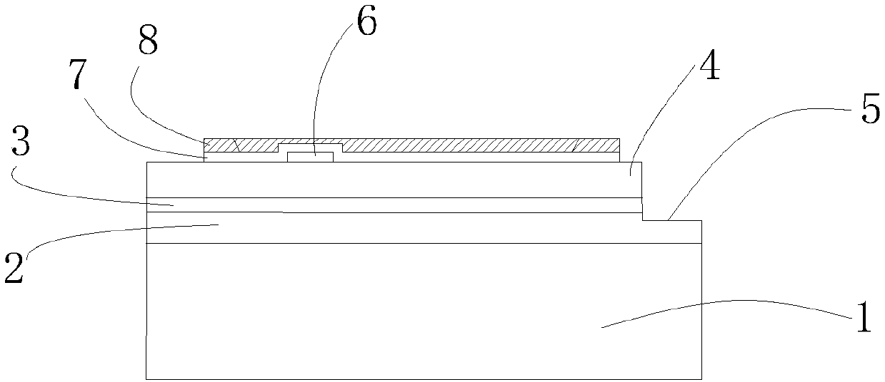
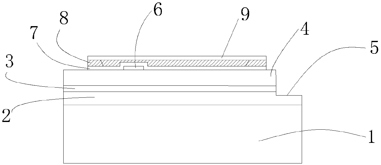
[0041] First, an LED chip body is provided. The main body of the LED chip includes a substrate 1 on which an N semiconductor layer 2 , a light emitting layer 3 and a P semiconductor layer 4 are sequentially formed. Parts of the P semiconductor layer 4 , the light emitting layer 3 and the N semiconductor layer 2 are etched away by a conventional MESA (platform), forming a gap 5 extending from the P semiconductor layer 4 to the N semiconductor layer 2 . Then, a current blocking layer 6 is formed by depositing and etching on a part of the P semiconductor layer 4 . Then, an indium tin oxide layer is deposited on the P semiconductor layer 4 by magnetron sputtering with a thickness of 40 nm, so that the indium tin oxide layer covers the current blocking layer 6 .
[0042] Then, the solid metal raw material Al is deposited on the indium tin oxide layer by vacuum evaporation to obtain a metal Al layer with a thickness of 2.5 nm, and then the metal Al layer is annealed to obtain a cry...
Embodiment 2
[0048] First, an LED chip body is provided. The main body of the LED chip includes a substrate 1 on which an N semiconductor layer 2 , a light emitting layer 3 and a P semiconductor layer 4 are sequentially formed. Parts of the P semiconductor layer 4 , the light emitting layer 3 and the N semiconductor layer 2 are etched away by a conventional MESA (platform), forming a gap 5 extending from the P semiconductor layer 4 to the N semiconductor layer 2 . Then, a current blocking layer 6 is formed by depositing and etching on a part of the P semiconductor layer 4 . Then, an indium tin oxide layer is deposited on the P semiconductor layer 4 by magnetron sputtering, with a thickness of 20 nm, so that the indium tin oxide layer covers the current blocking layer 6 .
[0049] Then the solid metal raw material Ni is deposited on the indium tin oxide layer by a sputtering deposition method to obtain a metal Ni layer with a thickness of 0.5nm, and then the metal Ni layer is annealed to o...
Embodiment 3
[0053] First, an LED chip body is provided. The main body of the LED chip includes a substrate 1 on which an N semiconductor layer 2 , a light emitting layer 3 and a P semiconductor layer 4 are sequentially formed. Parts of the P semiconductor layer 4 , the light emitting layer 3 and the N semiconductor layer 2 are etched away by a conventional MESA (platform), forming a gap 5 extending from the P semiconductor layer 4 to the N semiconductor layer 2 . Then, a current blocking layer 6 is formed by depositing and etching on a part of the P semiconductor layer 4 . Then, an indium tin oxide layer is deposited on the P semiconductor layer 4 by magnetron sputtering, with a thickness of 100 nm, so that the indium tin oxide layer covers the current blocking layer 6 .
[0054] Then, the solid metal raw material Ti is deposited on the indium tin oxide layer by a sputtering deposition method to obtain a metal Ti layer with a thickness of 5 nm, and then the metal Ti layer is annealed to ...
PUM
| Property | Measurement | Unit |
|---|---|---|
| thickness | aaaaa | aaaaa |
| thickness | aaaaa | aaaaa |
| thickness | aaaaa | aaaaa |
Abstract
Description
Claims
Application Information


