

Bipolar thermal activation delayed fluorescent material, preparation method thereof and organic electroluminescent diode device
A thermal activation delay, fluorescent material technology, applied in the direction of luminescent materials, electrical solid devices, chemical instruments and methods, etc., can solve the problems of unbalanced OLED turn-on voltage and life, single carrier transport properties, high turn-on voltage, etc. Achieve the effects of improving efficiency and stability, improving exciton utilization, and carrier transport balance
- Summary
- Abstract
- Description
- Claims
- Application Information
AI Technical Summary
Problems solved by technology
Method used
Image


Examples
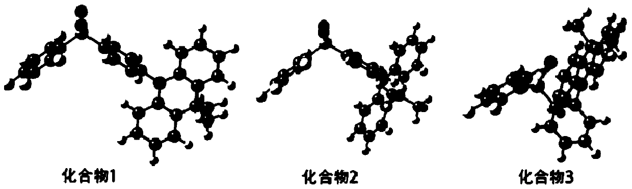
Embodiment 1
[0051] The synthetic route of target compound 1 is as follows:
[0052]
[0053] Add raw material 1 (1.93g, 5mmol), 9,10-dihydro-9,9-dimethylacridine (1.25g, 6mmol), palladium acetate Pb (OAc) (45mg, 0.2mmol) in 100mL two-necked flask ) and tri-tert-butylphosphine tetrafluoroborate (t-Bu) 3 HPBF 4 (0.17g, 0.6mmol), then add sodium tert-butoxide NaOt-Bu (0.58g, 6mmol) in the glove box, inject 40mL of toluene that has been dehydrated and deoxygenated in advance under an argon atmosphere, and react at 120°C for 24 hours . Cool to room temperature, pour the reaction solution into 200mL ice water, extract three times with dichloromethane, combine the organic phases, spin into silica gel, and separate and purify by column chromatography (dichloromethane:n-hexane, v:v, 3:2) to obtain 2.3 g of compound 1 as a white powder, yield 89%.
[0054] 1HNMR (300MHz, CD2Cl2, δ): 7.62(d, J=6.3Hz, 2H), 7.35(d, J=6.6Hz, 2H), 7.19-7.14(m, 6H), 6.95-6.90(m, 2H) ,1.69(s,6H).
[0055] MS(EI)m...
Embodiment 2
[0057] The synthetic route of target compound 2 is as follows:
[0058]
[0059] Add raw material 2 (1.93g, 5mmol), 9,10-dihydro-9,9-dimethylacridine (1.25g, 6mmol), palladium acetate (45mg, 0.2mmol) and three tert-tert Butylphosphine tetrafluoroborate (0.17g, 0.6mmol), then sodium tert-butoxide (0.58g, 6mmol) was added in the glove box, and 40mL of toluene, which had been dehydrated and deoxygenated in advance, was injected under an argon atmosphere. React at 120°C for 24 hours. Cool to room temperature, pour the reaction solution into 200mL ice water, extract three times with dichloromethane, combine the organic phases, spin into silica gel, and separate and purify by column chromatography (dichloromethane:n-hexane, v:v, 3:2) to obtain 1.7 g of compound 2 as white powder, yield 66%.
[0060] 1 H NMR (300MHz, CD 2 Cl 2 ,δ): 7.69 (d, J=6.0Hz, 1H), 7.52-7.44 (m, 3H), 7.19-7.14 (m, 6H), 6.95-6.90 (m, 2H), 1.69 (s, 6H).
[0061] MS(EI)m / z:[M] + calcd for C 27 h 18 f ...
Embodiment 3
[0063] The synthetic route of target compound 3 is as follows:
[0064]
[0065] Add raw material 3 (1.93g, 5mmol), 9,10-dihydro-9,9-dimethylacridine (1.25g, 6mmol), palladium acetate (45mg, 0.2mmol) and three tert-tert Butylphosphine tetrafluoroborate (0.17g, 0.6mmol), then sodium tert-butoxide (0.58g, 6mmol) was added in the glove box, and 40mL of toluene, which had been dehydrated and deoxygenated in advance, was injected under an argon atmosphere. React at 120°C for 24 hours. Cool to room temperature, pour the reaction solution into 200mL ice water, extract three times with dichloromethane, combine the organic phases, spin into silica gel, and separate and purify by column chromatography (dichloromethane:n-hexane, v:v, 3:2) to obtain 1.1 g of compound 3 as a white powder, yield 43%.
[0066] 1 H NMR (300MHz, CD 2 Cl 2 ,δ): 7.72 (d, J=6.3Hz, 2H), 7.35-7.29 (m, 3H), 7.19-7.14 (m, 6H), 6.95-6.90 (m, 2H), 1.69 (s, 6H).
[0067] MS(EI)m / z:[M] + calcd for C 27 h 18 f...
PUM
 Abstract
Description
Claims
Application Information