Rapid testing method for system-in-package module structure
A technology of system-level packaging and module structure, which is applied in the direction of electronic circuit testing, measuring electricity, and measuring devices, and can solve the problems of unable to fit probes, high density, and increased test time
- Summary
- Abstract
- Description
- Claims
- Application Information
AI Technical Summary
Problems solved by technology
Method used
Image


Examples
Embodiment 1
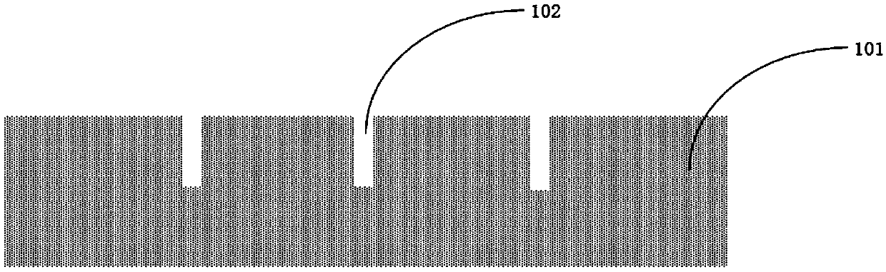
[0034] Such as Figure 1 to Figure 8 As shown, a rapid testing method for a system-in-package module structure, the specific processing includes the following steps:
[0035] 101) Processing steps of the test board 101: making TSV holes 102 on the upper surface of the test board 101 through photolithography and etching processes. The diameter of the TSV holes 102 ranges from 1um to 1000um, and the depth ranges from 10um to 1000um. An insulating layer is formed on the upper surface of the test board 101 by depositing silicon oxide or silicon nitride or direct thermal oxidation, and the thickness of the insulating layer ranges from 10 nm to 100 um. The seed layer is made on the insulating layer by physical sputtering, magnetron sputtering or evaporation process. The thickness of the seed layer ranges from 1nm to 100um. The seed layer structure adopts one or more layers. The metal material of the seed layer is titanium, copper, One or more of aluminum, silver, palladium, gold, t...
Embodiment 2
[0045] Such as Figure 7 to Figure 13 As shown, a rapid testing method for the system-in-package module structure, the specific processing includes the following steps:
[0046] 101) Processing steps of the test board 101: making TSV holes 102 on the upper surface of the test board 101 through photolithography and etching processes, the diameter of the TSV holes 102 ranges from 1um to 1000um, and the depth ranges from 10um to 1000um. An insulating layer is formed on the upper surface of the test board 101 by depositing silicon oxide or silicon nitride or direct thermal oxidation, and the thickness of the insulating layer ranges from 10nm to 100um. The seed layer is made on the insulating layer by physical sputtering, magnetron sputtering or evaporation process. The thickness of the seed layer ranges from 1nm to 100um. The seed layer structure adopts one or more layers. The metal material of the seed layer is titanium, copper, One or more of aluminum, silver, palladium, gold, ...
PUM
| Property | Measurement | Unit |
|---|---|---|
| Thickness | aaaaa | aaaaa |
| Thickness | aaaaa | aaaaa |
| Height | aaaaa | aaaaa |
Abstract
Description
Claims
Application Information
PatSnap Eureka turns technology decisions into work you can execute. Powered by our Innovation Knowledge Graph, it runs expert workflows across engineering, life sciences, materials and intellectual property. Get your review-ready output in minutes.


