System in package

a technology of system and package, applied in the field of system in package, can solve the problems of poor methods of testing the completed assembly, poor methods of die replacement, and existing stacked die package and system in package approaches, and achieve the effects of effective cooling of sip, high density, and high speed

Inactive Publication Date: 2005-08-25
SALMON TECH
View PDF99 Cites 45 Cited by
  • Summary
  • Abstract
  • Description
  • Claims
  • Application Information

AI Technical Summary

Benefits of technology

[0013] The current invention provides improvements in the following areas: higher levels of integration within a single SEP, an effective method for testing the completed assembly including a full speed functional test, e

Problems solved by technology

However, existing stacked die packages and system in package (SIP) approaches have suffered from poor methods of testing the completed assembly and poor methods for replacing any die that prove defective.
This has led to a relatively high cost of SIP solutions to date.
In addition, current stacked die packages have poor thermal performance and this has limited the level of integration attainable.
In particular, since most of the heat in current packages flows to the board on which the SIP is mounted, the top chips in a stack may get overheated.
These problems include the inability to align more than two stacked layers with fine alignment accuracy such as ±2 microns layer to layer; and the inability to pattern multiple dielectric layers by hot embossing when all of the layers are comprised of the same material, softening at the same temperature.
An additional problem addressed herein is difficulty in separating the embossing tool from the imprinted substrate; this problem is addressed using the method of vapor-assisted release.
Because the bump height varies, some bumps do not touch the corresponding lands and this can lead to poor solder connections.
Also, the mechanical attachment is

Method used


Image

  • System in package
  • System in package
  • System in package

Examples


Embodiment Construction

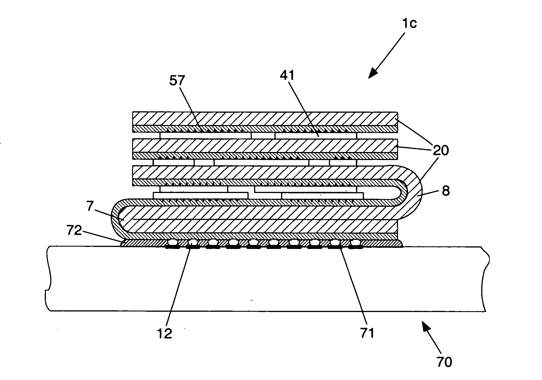
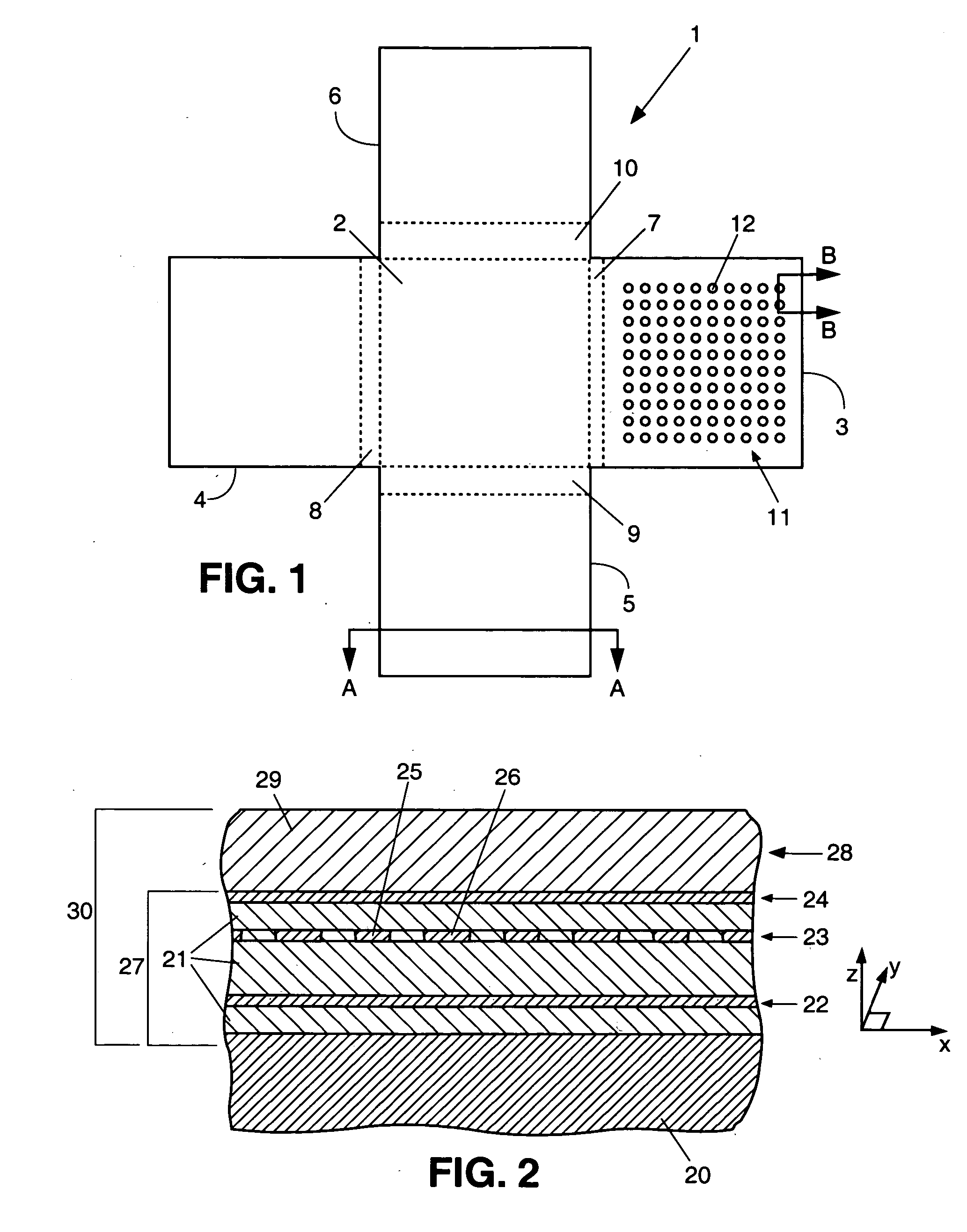
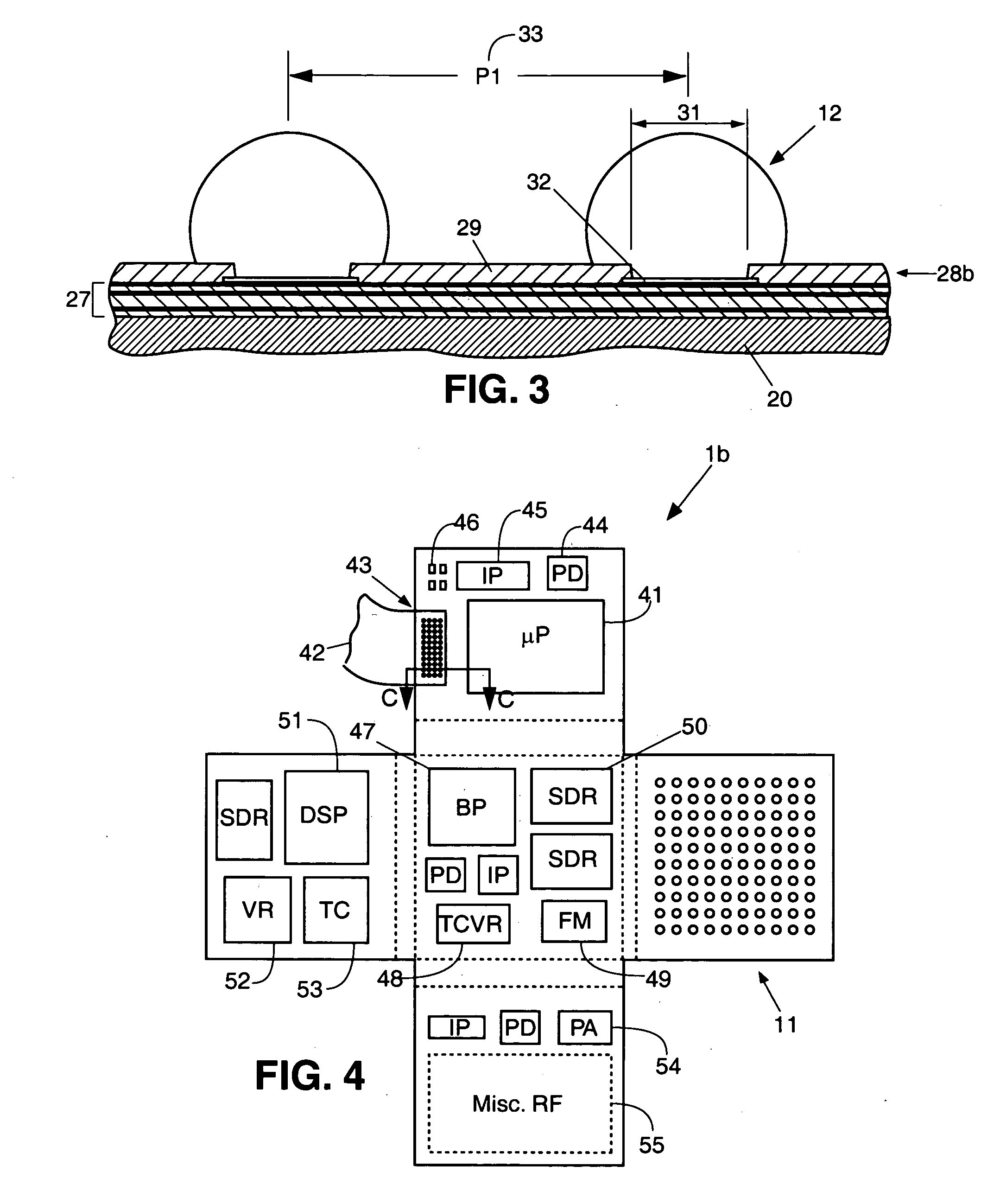
[0063]FIG. 1 is a top view of a foldable circuit board 1 of the current invention with five delineated surfaces including a center surface 2 and four tab-like surfaces 3-6 arranged around it. Rectangular areas 7-10 are reserved for hinges in the folded assembly. The first tab folded 3 will require a small hinge area 7 and the last tab folded 6 will require a larger hinge area 10 because the total thickness of the stacked layers (folded surfaces) increases with each additional folded surface. Tab surface 3 includes an array 11 of bump terminals 12 for connection to a printed circuit board, including provisions for signals and / or power. The array 11 of bumps 12 is one form of attachment site, in this case for attaching the SIP to a circuit board.

[0064]FIG. 2 illustrates a fragment of cross-section AA of FIG. 1, expanded to show a preferred layer structure. A substrate of conductive material 20, preferably copper or an alloy of copper supports multiple conductive and dielectric layers...


PUM


Abstract

A system in package (SIP) is fabricated on a sheet of copper foil. An interconnection circuit is fabricated on the foil using copper conductors and a dual damascene structure for each conductive layer. The preferred dielectric material is an amorphous fluorinated polymer called Cytop. Input/output traces of the interconnection circuit terminate in wells filled with solder. Chips are bumped and direct attached by inserting the bumps into the wells. The preferred bumps are gold stud bumps, and the preferred wells contain solder paste to a depth of approximately 15 microns. Imprinting is the preferred method for patterning; it enables 6-micron wide traces, 6-micron diameter vias, and a cost per well of around 0.02 cents. Stripline structures are described for a 4-layer stackup that can support operating frequencies of at least 10 GHz. New methods are proposed for testing the completed assembly and for rework of any chips that prove defective. After the assembly is fully tested and reworked in sheet form the copper foil is folded to form a stacked die package or system in package. 5-high and 9-high stacks are illustrated. The copper foil provides a low impedance thermal path for cooling every chip in the SIP.

Description

THE INVENTION [0001] This invention relates to microelectronic assemblies, and more particularly to semiconductor chip assemblies in which several layers of chips are stacked in a single package. BACKGROUND OF THE INVENTION [0002] A common approach to reducing cost and increasing performance of microelectronic systems is to provide higher levels of integration. This can be accomplished by creating more complex integrated circuit (IC) chips, or by integrating the chips more effectively into packages or onto system boards. For more effective integration of chips into packages, stacked die packages have been developed. However, existing stacked die packages and system in package (SIP) approaches have suffered from poor methods of testing the completed assembly and poor methods for replacing any die that prove defective. This has led to a relatively high cost of SIP solutions to date. In addition, current stacked die packages have poor thermal performance and this has limited the level ...

Claims


Application Information

Patent Timeline
IPC IPC(8): H01L21/00H01L21/48H01L21/66H01L23/367H01L23/498H01L23/538H01L25/065H01L25/18H05K1/05H05K1/18H05K3/20
CPCH01L22/22H01L2224/814H01L23/49894H01L23/5383H01L23/5386H01L23/5387H01L25/0652H01L25/18H01L2223/6627H01L2223/6638H01L2223/6677H01L2224/16237H01L2924/19032H01L2924/19105H01L2924/3011H05K1/056H05K1/189H05K3/20H01L21/4867H01L21/67092H01L2924/01087H01L2924/01322H01L23/3675H01L2224/81191H01L2924/014H01L2224/05568H01L2224/05573H01L2924/00014H01L2224/05599
Inventor SALMON, PETER C.
Owner SALMON TECH
Why Eureka
Try Eureka