Method for manufacturing silicon cavity structure with TSV structure at bottom
A manufacturing method and cavity technology, which are applied in semiconductor/solid-state device manufacturing, electrical components, circuits, etc., can solve the problems of high cost, unfavorable chip grounding interconnection, and bottom inequality, and achieve simple manufacturing process, cost saving and manufacturing time. Effect
- Summary
- Abstract
- Description
- Claims
- Application Information
AI Technical Summary
Problems solved by technology
Method used
Image
Examples
Embodiment 1
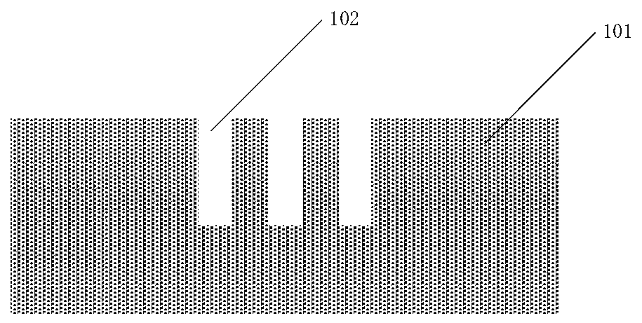
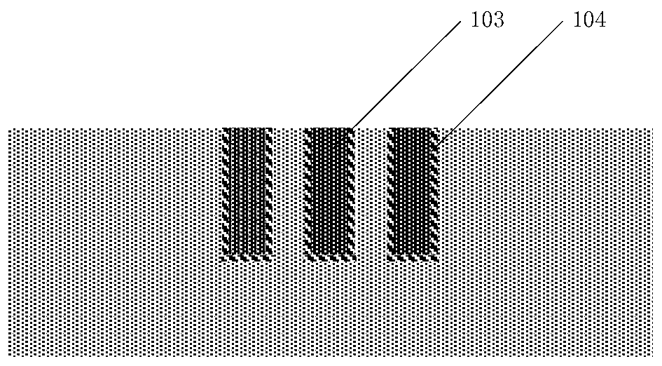
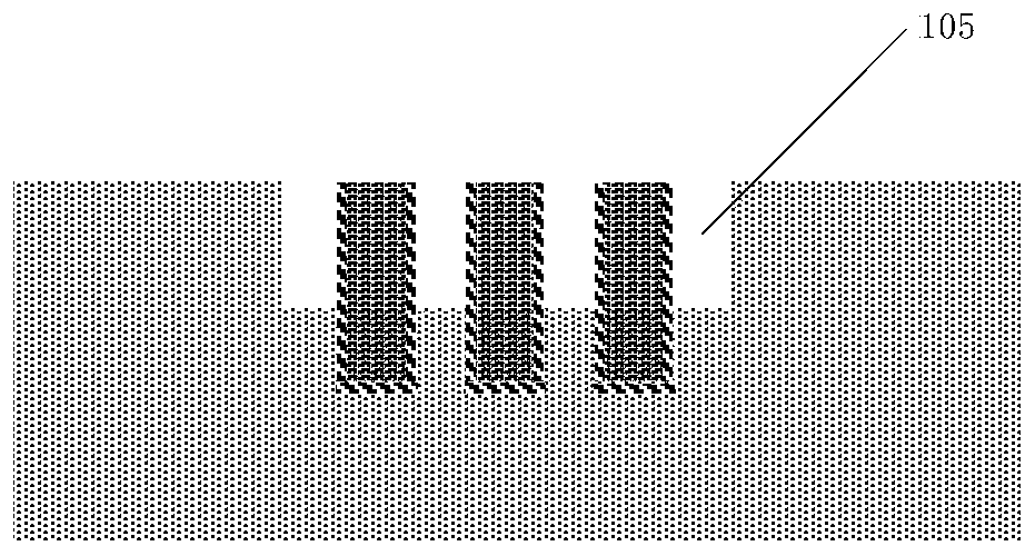
[0035] A method for manufacturing a silicon cavity 105 structure with a TSV structure at the bottom, the specific processing includes the following steps:
[0036] 101) The step of making metal pillars 103: making TSV holes 102 on the surface of the carrier 101, the depth of the TSV holes 102 is smaller than the thickness of the carrier, and filling the TSV holes 102 with metal. Such as figure 1 As shown, TSV holes 102 are formed on the upper surface of the carrier 101 by photolithography and etching processes. The TSV holes 102 have a diameter ranging from 1um to 1000um and a depth ranging from 10um to 1000um.
[0037] Such as figure 2 As shown, an insulating layer 104 such as silicon oxide or silicon nitride is deposited on the silicon wafer, or directly thermally oxidized, and the thickness of the insulating layer 104 ranges from 10 nm to 100 um. A seed layer is formed on the insulating layer 104 by physical sputtering, magnetron sputtering or evaporation process. The th...
Embodiment 2
[0046] It is basically the same as Embodiment 1, except that step 102) uses a dry etching process to make the area of the TSV hole 102 on the upper surface of the carrier 101, and after performing dry etching to form the cavity 105, because the insulating layer will be damaged 104 , the insulating layer 104 may be formed again on the carrier 101 . The generation method is the same as the first time, and the thickness range of the insulating layer 104 this time is still between 10nm and 100um.
Embodiment 3
[0048] It is basically the same as Embodiment 1, the difference lies in step 102). Such as Figure 6 to Figure 8 As shown, in embodiment three, the dry etching process is used to thin the lower surface of the carrier plate 101, and the thickness of the thinning is from 100nm to 700um. The bonding process protects the surface of the carrier plate 101 on which the TSV holes 102 are provided, and then uses the temporary bonding process to protect the carrier sheet as a support to thin the lower surface of the carrier plate 101 .
[0049] In the area corresponding to the TSV hole 102, dry etching or wet etching is performed to form a cavity 105, the width of the cavity 105 is larger than the area of the TSV hole 102, and the copper pillar is exposed. An insulating layer 104 is formed on the lower surface of the carrier 101 by deposition or direct thermal oxidation, and the insulating layer 104 on the surface of the copper pillars is removed by wet etching or dry etching.
PUM
| Property | Measurement | Unit |
|---|---|---|
| Thickness | aaaaa | aaaaa |
| Thickness | aaaaa | aaaaa |
| Thickness | aaaaa | aaaaa |
Abstract
Description
Claims
Application Information
 - R&D
- Intellectual Property
- Life Sciences
- Materials
- Tech Scout
- Unparalleled Data Quality
- Higher Quality Content
- 60% Fewer Hallucinations
Browse by: Latest US Patents, China's latest patents, Technical Efficacy Thesaurus, Application Domain, Technology Topic, Popular Technical Reports.
© 2025 PatSnap. All rights reserved.Legal|Privacy policy|Modern Slavery Act Transparency Statement|Sitemap|About US| Contact US: help@patsnap.com


