Non-polar ALGAN-based Schottky UV detector

A non-polar and detector technology, applied in semiconductor devices, photovoltaic power generation, electrical components, etc., can solve the problem of low photoelectric conversion efficiency of detectors, lattice mismatch, and limitations on the performance and development of Schottky ultraviolet detectors, etc. question

Active Publication Date: 2019-08-23
SOUTHEAST UNIV
View PDF7 Cites 2 Cited by
  • Summary
  • Abstract
  • Description
  • Claims
  • Application Information

AI Technical Summary

Problems solved by technology

[0004] However, if image 3 In the traditional polar AlGaN-based Schottky UV detector shown, due to the presence of a polarized electric field with an intensity as high as MV/cm in the direction parallel to the incident light, the photogenerated carriers in the ohmic contact layer are perpendicular to The lateral movement of the polarization electric field to the corresponding electrode will be strongly hindered by the polarization electric field, so that the photoelectric conversion efficiency of the detector is not high
In addition, during the growth process o...

Method used


Image

  • Non-polar ALGAN-based Schottky UV detector
  • Non-polar ALGAN-based Schottky UV detector
  • Non-polar ALGAN-based Schottky UV detector

Examples


Embodiment 1

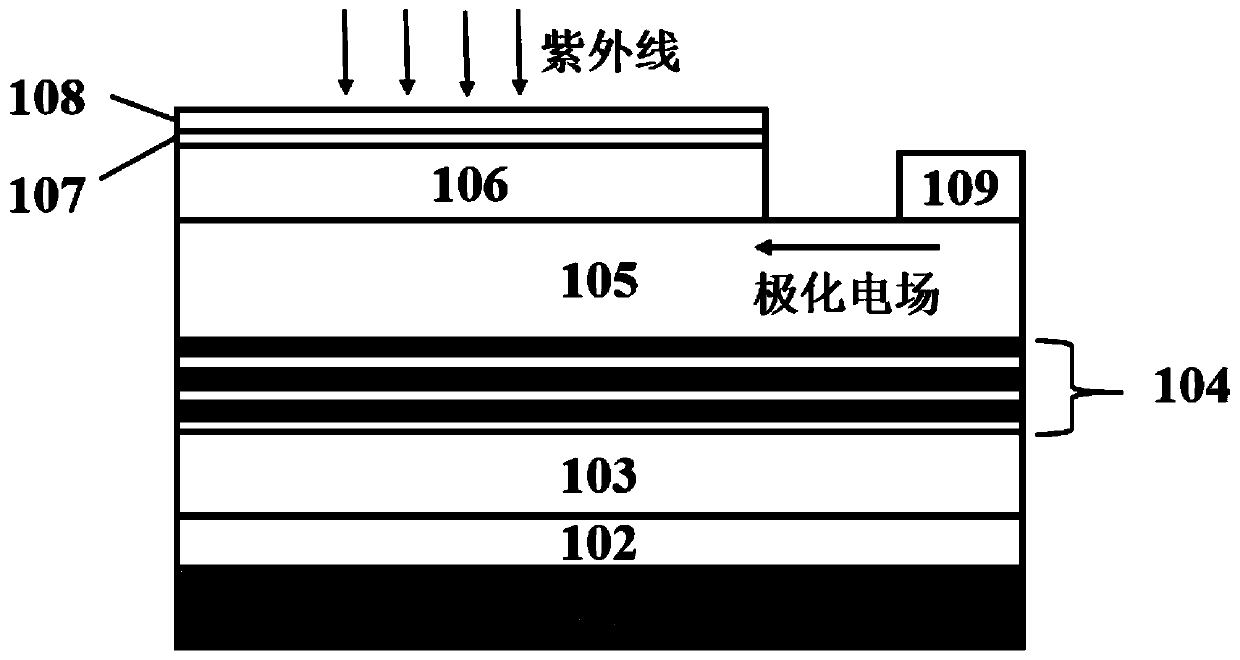
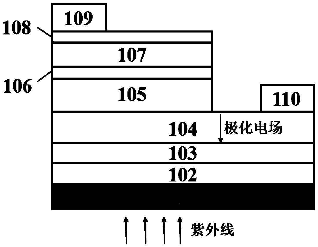
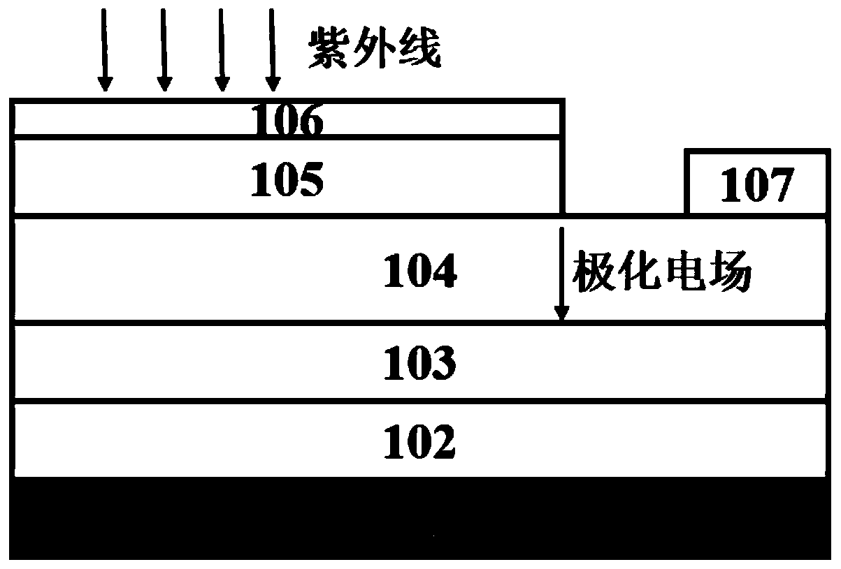
[0018] figure 1 Shown is a non-polar AlGaN-based Schottky ultraviolet detector provided by the present invention, including a substrate (101), a low-temperature AlN nucleation layer (102), and a high-temperature AlN buffer layer (103) arranged in sequence from bottom to top , AlN / Al 0.6 Ga 0.4 N superlattice structure (104), n-type doped n-Al 0.3 Ga 0.7 N layer (105), n-type doped n-Al 0.38 Ga 0.62 N absorption layer (106), AlN barrier enhancement layer (107), metal thin film layer (108), in n-Al 0.3 Ga 0.7 Ohmic electrodes (109) are drawn out from the N layer (105). Except for the substrate (101), metal thin film layer (108) and ohmic electrode (109), all other layers are made of non-polar AlGaN base material.

[0019] The metal thin film layer (108) and the ohmic electrode (109) are respectively located at the negative and positive poles of the transverse polarization electric field.

[0020] The material of the metal thin film layer (108) is Au, and its work funct...

Embodiment 2

[0028] figure 1 Shown is a non-polar AlGaN-based Schottky ultraviolet detector provided by the present invention, including a substrate (101), a low-temperature AlN nucleation layer (102), and a high-temperature AlN buffer layer (103) arranged in sequence from bottom to top , AlN / Al 0.6 Ga 0.4 N superlattice structure (104), n-type doped n-Al 0.3 Ga 0.7 N layer (105), n-type doped n-Al 0.38 Ga 0.62 N absorption layer (106), AlN barrier enhancement layer (107), metal thin film layer (108), in n-Al 0.3 Ga 0.7 Ohmic electrodes (109) are drawn out from the N layer (105). Except for the substrate (101), metal thin film layer (108) and ohmic electrode (109), all other layers are made of non-polar AlGaN base material.

[0029] The metal thin film layer (108) and the ohmic electrode (109) are respectively located at the negative and positive poles of the transverse polarization electric field.

[0030] The material of the metal thin film layer (108) is Au, and its work funct...

Embodiment 3

[0035] figure 1 Shown is a non-polar AlGaN-based Schottky ultraviolet detector provided by the present invention, including a substrate (101), a low-temperature AlN nucleation layer (102), and a high-temperature AlN buffer layer (103) arranged in sequence from bottom to top , AlN / Al 0.6 Ga 0.4 N superlattice structure (104), n-type doped n-Al 0.3 Ga 0.7 N layer (105), n-type doped n-Al 0.38 Ga 0.62 N absorption layer (106), AlN barrier enhancement layer (107), metal thin film layer (108), in n-Al 0.3 Ga 0.7 Ohmic electrodes (109) are drawn out from the N layer (105). Except for the substrate (101), metal thin film layer (108) and ohmic electrode (109), all other layers are made of non-polar AlGaN base material.

[0036] The metal thin film layer (108) and the ohmic electrode (109) are respectively located at the negative and positive poles of the transverse polarization electric field.

[0037] The material of the metal thin film layer (108) is Au, and its work funct...


PUM

PropertyMeasurementUnit
Thicknessaaaaaaaaaa
Thicknessaaaaaaaaaa
Thicknessaaaaaaaaaa

Abstract

The invention provides a non-polar ALGAN-based Schottky UV detector. The non-polar ALGAN-based Schottky UV detector is sequentially provided with a substrate, a low temperature AlN nucleation layer, ahigh temperature AlN buffer layer, an AlN/AlxGa1-xN superlattice structure, an n-type doped n-AlyGa1-yN layer, an n-type doped n-AlzGa1-zN absorption layer, an AlN barrier enhancement layer and a metal film layer from bottom to top, wherein an ohmic electrode is extracted in the n-AlyGa1-yN layer, and o<y<z<x<1. The detector is advantaged in that as the non-polar n-AlyGa1-yN layer has a laterallypolarized electric field directed from an anode to a cathode, photogenerated carriers in the n-AlyGa1-yN layer are accelerated to migrate to the ohmic electrode, photocurrent generation efficiency isgreatly improved, and thereby photoelectric conversion efficiency and responsiveness of the device are improved; the AlN/AlxGa1-xN superlattice structure is inserted, buffer layer barrier height is increased, and crystal quality of the AlGaN epitaxial layer is improved; the AlN barrier enhancement layer is interposed between the n-AlzGa1-zN absorption layer and the metal film layer, height and thickness of a Schottky barrier can effectively be increased, through insertion of the AlN/AlxGa1-xN superlattice structure and the AlN barrier enhancement layer, reducing the dark current of the deviceis facilitated, and the signal-to-noise ratio and stability of the detector are improved.

Description

technical field [0001] The invention relates to the field of semiconductor optoelectronic devices, in particular to a non-polar AlGaN-based Schottky ultraviolet detector. Background technique [0002] With the vigorous development of third-generation semiconductor materials such as GaN, diamond and SiC, it will lay the foundation for the development of high-performance ultraviolet detectors. Especially AlGaN material, because its forbidden band width can be adjusted between 3.4-6.2 eV by controlling the aluminum composition, and the corresponding spectral wavelength covers the ultraviolet region of 365-200 nm, so it has significant advantages in ultraviolet detection. It is an ideal material for making ultraviolet photodetection devices. [0003] At present, most of the ultraviolet detectors used in the market are such as figure 2 The p-n junction or pin structure shown is usually back-illuminated. Compared with these traditional UV detectors, Schottky UV detectors have u...

Claims


Application Information

Patent Timeline
IPC IPC(8): H01L31/0304H01L31/108
CPCH01L31/03044H01L31/03048H01L31/108Y02E10/544
Inventor 张雄饶立锋崔一平
Owner SOUTHEAST UNIV
Why Eureka
Try Eureka