Micro force sensor integrated with sensitive membrane and force transmission guiding rod and processing method thereof

A technology of micro force sensor and force transmission guide rod, which is applied in the field of sensors, can solve the problems of reducing force transmission sensitivity, cumbersome installation, and difficulty, and achieve the effects of simplifying the preparation process and installation process, improving measurement accuracy, and eliminating installation errors

Active Publication Date: 2019-09-06
SHANGHAI INST OF TECH
View PDF9 Cites 4 Cited by
  • Summary
  • Abstract
  • Description
  • Claims
  • Application Information

AI Technical Summary

Problems solved by technology

[0004] The traditional method of testing the pressure-sensitive sensor is usually prepared separately from the pressure-sensitive sensor and the force-transmitting rod, and the pressure-sensitive sensor and the force-transmitting rod are connected through an adhesive. It is very difficult, and it is easy to affect the force conduction in the follow-up measurement work of the pressure-sensitive sensor. For the delicate components of the sensor, it is easy to cause measurement errors
Ritsumeikan University Dzung et al. prepared a micro force sensor for measuring robot finger force in 2006 through microfabrication (see "SIX-DEGREE OF FREEDOM MICRO FORCE-MOMENTSENSOR FOR APPLICATION IN GEOPHYSICS" 2002 Proceedings of the IEEEInternational Conference on Micro Electro Mechanical Systems (MEMS) February 2002, pp.312-315), but the installation between the pressure-sensitive sensor and the force transmission rod is cumbersome during the test process and the force transmission is easily affected and causes errors, so it is not suitable for mass production
[0005] Chinese patent CN104729784 A discloses a beam-groove combined stepped island membrane micro-pressure sensor chip and its preparation method. The chip includes a thin film in the middle of the base, four shallow grooves are distributed along the upper edge of the thin film, and four relief beams are arranged on adjacent two shallow Between the ends of the grooves and the base, the upper surface of the embossed beam, the upper surface of the film and the bottom surface of the shallow groove form a beam-groove combined stepped film structure. Four piezoresistor strips are arranged on the four embossed beams. Metal leads The varistor strips are connected to form a semi-open-loop Wheatstone bridge, and the output end of the bridge is connected to the pad; the four bumps are evenly distributed along the lower edge of the film and connected to the substrate; the four mass blocks are spaced from the bumps by distance, the bumps are connected on the film, and the preparation method is to oxidize the SOI silicon wafer at high temperature to make a varistor strip, obtain the ohmic contact area to make metal leads and pads; then make four embossed beams and shallow grooves, and finally connect the back of the substrate with the anti- Overload glass bonding; however, this patented technology is a traditional piezoresistor structure, and the force acts directly on the piezoresistor, which limits the application field of the sensor and reduces the sensitivity of force transmission

Method used


Image

  • Micro force sensor integrated with sensitive membrane and force transmission guiding rod and processing method thereof
  • Micro force sensor integrated with sensitive membrane and force transmission guiding rod and processing method thereof
  • Micro force sensor integrated with sensitive membrane and force transmission guiding rod and processing method thereof

Examples


Embodiment 1

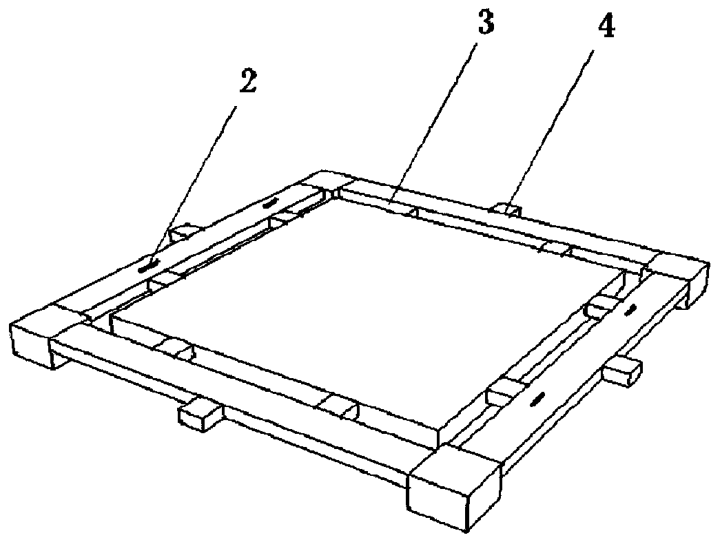
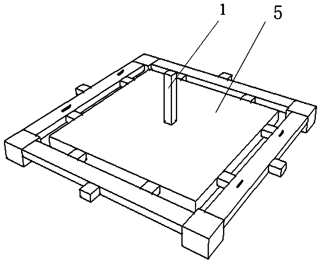
[0033] This embodiment provides a micro force sensor integrated with a sensitive membrane and a force transmission guide rod, including a fixedly connected sensitive membrane and a force transmission guide rod 1 . Such as figure 1 As shown, the sensitive film includes a central plate 5, a cantilever beam connected around the central plate 5, and a piezoresistor 2 arranged on the cantilever beam 4, and metal leads connect the piezoresistors to each other to form a Wheatstone bridge; among them, such as figure 1 As shown, the cantilever beam 4 includes four load beams 41 parallel to the edge of the center plate 5 and a connecting beam 42 connected between the load beams 41 and the center plate 5; each load beam 41 is connected to the center plate through two connecting beams 42 5 connections, each of the four load beams 41 is provided with two piezoresistors 2, so there are eight piezoresistors 2 in this embodiment; the load beams 41 are provided with contact holes matching the...

Embodiment 2

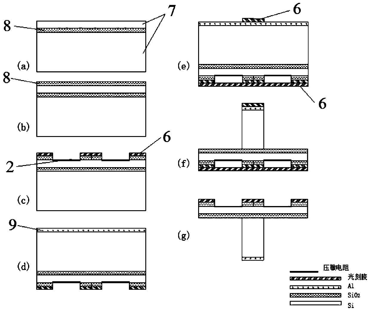
[0039] This embodiment provides a method for manufacturing the micro force sensor with the structure of Embodiment 1, the processing process is as follows image 3 As shown, the method includes the following steps:

[0040] 1. Processing of varistor 2

[0041] Select a 1mm thick SOI silicon wafer, clean and dry it. The silicon wafer includes a front monocrystalline silicon with a thickness of 30 μm, a silicon dioxide buried layer and a 950 μm rear monocrystalline silicon, in which the monocrystalline silicon is all N type monocrystalline silicon, such as image 3 (a) Si 7-SiO shown 2 The structure of 8-Si 7 is cleaned and dried; a 0.3um silicon dioxide film is formed on the front single crystal silicon of the SOI silicon wafer by thermal oxidation, such as image 3 SiO shown in (b) 2 8 structure; use the varistor plate to photoetch the varistor area on the silicon dioxide film, remove the silicon dioxide film in the varistor area on the silicon dioxide film, and expose t...

Embodiment 3

[0048] This embodiment is a micro-force sensor integrated with a sensitive film and a force transmission guide rod. Its main structure is the same as that of Embodiment 1, except that the force transmission guide rod is a cylindrical structure.

[0049] The specification parameters of the SOI silicon wafer used in the preparation process are: the thickness of the SOI silicon wafer is 0.5 mm, the thickness of the front monocrystalline silicon is 30 μm, and the thickness of the rear monocrystalline silicon is 400 μm.


PUM

PropertyMeasurementUnit
thicknessaaaaaaaaaa
thicknessaaaaaaaaaa
thicknessaaaaaaaaaa

Abstract

The invention relates to a micro force sensor integrated with a sensitive membrane and a force transmission guiding rod. The sensor comprises a sensitive membrane and a force transmission guiding rodthat are fixedly connected. The sensitive membrane includes a substrate, a central plate disposed at the central position of the substrate, a cantilever beam connected between the substrate and the central plate, and a piezoresistor arranged on the cantilever beam. A contact hole matching the piezoresistor is formed in the substrate; and a metal lead and the piezoresistor form ohmic contact in thecontact hole and form a Wheatstone bridge. The central plate is connected to the force transmission guiding rod in an integrated manner. Compared with the prior art, the micro force sensor has advantages of simple preparation, low cost, small measurement error, great convenience in installation and the like.

Description

technical field [0001] The invention relates to the technical field of sensors, in particular to a micro force sensor integrating a sensitive film and a force transmission guide rod and a processing method thereof. Background technique [0002] With the advent of the new technology revolution, the world has entered the information age, and sensors, as the main way and means to obtain information in the fields of nature and production, have played a great role. Some weaknesses in our country's sensor testing process are inevitably revealed, such as certain improvements in the testing of pressure-sensitive sensors. [0003] For this reason, the present invention designs a micro force sensor in which a sensitive film and a force transmission guide rod are integrally prepared. The micro force sensor is a device made by spreading resistance on the substrate of the semiconductor material according to the piezoresistive effect of the semiconductor material. The basic principle is...

Claims


Application Information

Patent Timeline
Patent Type & Authority Applications(China)
IPC IPC(8): G01L1/18G01L9/06
CPCG01L1/18G01L9/06
Inventor 李以贵金敏慧王欢张成功王洁蔡金东
Owner SHANGHAI INST OF TECH
Why Eureka
Try Eureka