Multifunctional acoustic surface wave sensor and preparation method and application thereof
A surface acoustic wave and sensor technology, used in the analysis of fluids using sonic/ultrasonic/infrasonic waves, material analysis using sonic/ultrasonic/infrasonic waves, instruments, etc. It can solve the problems of complex operation process and long cycle.
- Summary
- Abstract
- Description
- Claims
- Application Information
AI Technical Summary
Problems solved by technology
Method used
Image
Examples
Embodiment 1
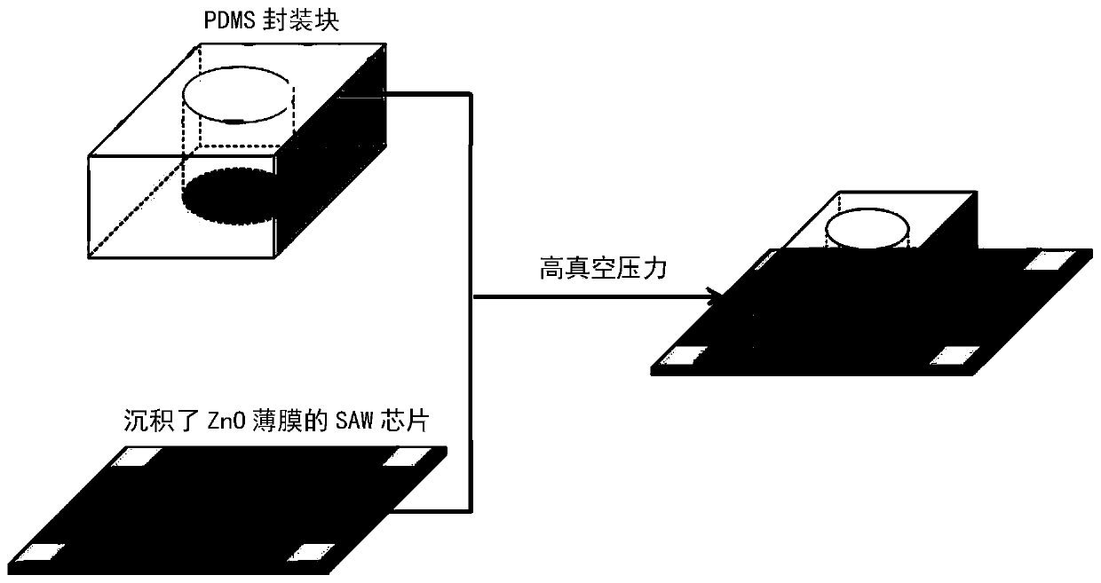
[0023] A preparation method of a multifunctional surface acoustic wave sensor, the steps are as follows:
[0024] S1. Preparation of SAW chip: select a piezoelectric substrate, and prepare interdigitated electrodes on the piezoelectric substrate through a photolithography micromachining process;
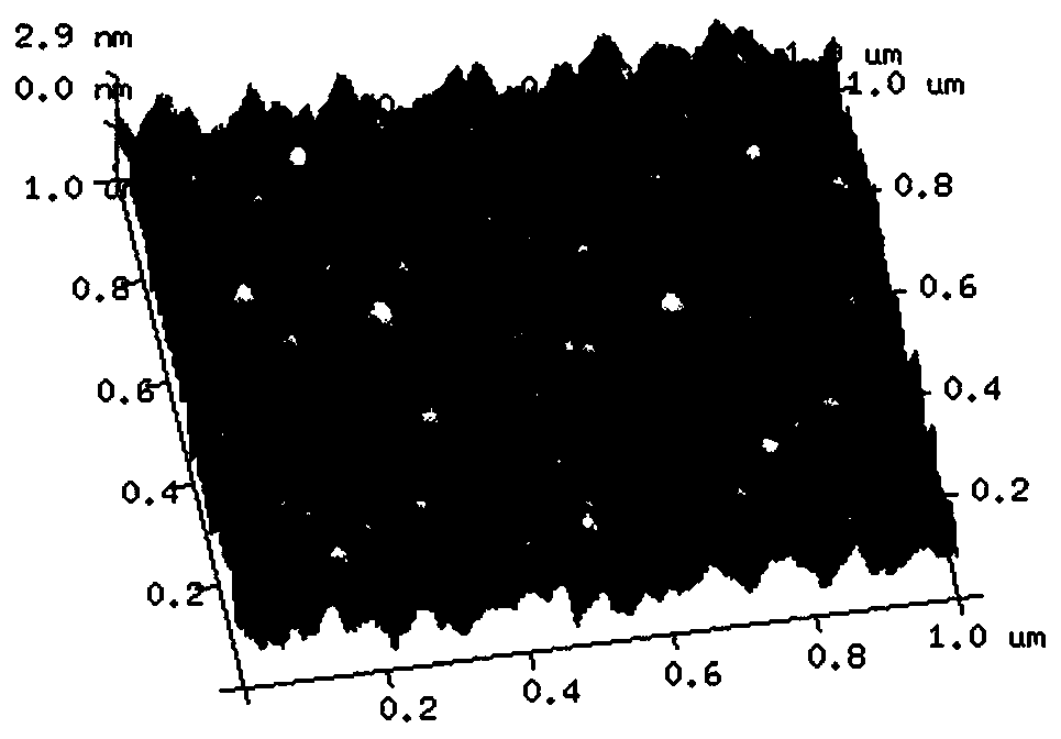
[0025] S2. Deposit ZnO thin film: on the surface of the SAW chip, deposit a nano-particle ZnO thin film with a size of 25-45nm by magnetron sputtering; Control the difference of sputtering parameters to control the morphology of the ZnO thin film deposited on the surface of the SAW chip. Sputtering, magnetron sputtering deposition ZnO thin film is deposited in two layers, after the first layer is deposited, wait for the temperature to drop to 65°C, and start the second layer deposition; the deposition parameters of the first layer are: the coating vacuum is 0.5Pa, the sputtering The sputtering power is 50W, and the sputtering time is 60min; the deposition parameters of the second la...
Embodiment 2
[0035] A preparation method of a multifunctional surface acoustic wave sensor, the steps are as follows:
[0036] S1. Preparation of SAW chip: select a piezoelectric substrate, and prepare interdigitated electrodes on the piezoelectric substrate through a photolithography micromachining process;
[0037] S2. Deposit ZnO thin film: on the surface of the SAW chip, deposit a nano-particle ZnO thin film with a size of 25-45nm by magnetron sputtering; Control the difference of sputtering parameters to control the morphology of the ZnO thin film deposited on the surface of the SAW chip. Sputtering, magnetron sputtering deposition ZnO thin film is deposited in two layers, after the first layer is deposited, wait until the temperature drops to 50°C, and start the second layer deposition; the deposition parameters of the first layer are: the coating vacuum is 0.4Pa, the sputtering The sputtering power is 40W, and the sputtering time is 70min; the deposition parameters of the second la...
Embodiment 3
[0045] A preparation method of a multifunctional surface acoustic wave sensor, the steps are as follows:
[0046] S1. Preparation of SAW chip: select a piezoelectric substrate, and prepare interdigitated electrodes on the piezoelectric substrate through a photolithography micromachining process;
[0047] S2. Deposit ZnO thin film: on the surface of the SAW chip, deposit a nano-particle ZnO thin film with a size of 25-45nm by magnetron sputtering; Control the difference of sputtering parameters to control the morphology of the ZnO thin film deposited on the surface of the SAW chip. Sputtering, magnetron sputtering deposition ZnO thin film is deposited in two layers, after the first layer is deposited, the temperature drops to 80°C, and the second layer deposition starts; the deposition parameters of the first layer are: the coating vacuum is 0.6Pa, the sputtering The sputtering power is 60W, and the sputtering time is 50min; the deposition parameters of the second layer are: t...
PUM
| Property | Measurement | Unit |
|---|---|---|
| width | aaaaa | aaaaa |
| thickness | aaaaa | aaaaa |
Abstract
Description
Claims
Application Information
 - R&D
- Intellectual Property
- Life Sciences
- Materials
- Tech Scout
- Unparalleled Data Quality
- Higher Quality Content
- 60% Fewer Hallucinations
Browse by: Latest US Patents, China's latest patents, Technical Efficacy Thesaurus, Application Domain, Technology Topic, Popular Technical Reports.
© 2025 PatSnap. All rights reserved.Legal|Privacy policy|Modern Slavery Act Transparency Statement|Sitemap|About US| Contact US: help@patsnap.com


