

Process method for preparing acid corrosion wafer with high brightness at single side
A process method and high-brightness technology, applied in the fields of semiconductor/solid-state device manufacturing, electrical components, circuits, etc., can solve problems such as the inability to achieve stable mass production, save the cost of main materials and chemical consumption, reduce thickness, and save costs and working hours
- Summary
- Abstract
- Description
- Claims
- Application Information
AI Technical Summary
Problems solved by technology
Method used
Image

Examples
Embodiment
[0034] Process preparation:
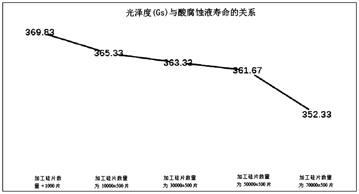
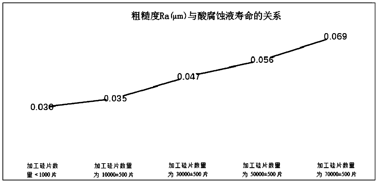
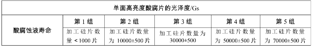
[0035] 1. Preparation of test pieces: 6-inch zone-fused double-sided grinding pieces, diameter 150±0.2mm, thickness: 550±5μm, resistivity: 60-80Ω·cm, quantity: 300 pieces, divide 300 pieces of double-sided grinding pieces into 5 Groups, 60 tablets per group.
[0036] 2. Test equipment: gloss meter, dial indicator, fluorescent lamp, microscope;
[0037] 3. Main processing equipment and tooling: grinding machine, 2000# grinding wheel, acid rot machine, cleaning machine;
[0038] 4. Acid corrosion solution: hydrofluoric acid solution: nitric acid solution: acetic acid solution = 1:4:1.8 (volume ratio); the HF content in the hydrofluoric acid solution is 49%wt, and the HNO in the nitric acid solution 3 Content is 70%wt, CH in acetic acid solution 3 The COOH content is 99.5%wt.
[0039] 5. Acid corrosion temperature: 30±2℃;
[0040] The process of preparing single-sided high-brightness acid-rot sheet is as follows:
[0041] 1) Single-side shear g...
PUM
| Property | Measurement | Unit |
|---|---|---|
| gloss | aaaaa | aaaaa |
| surface roughness | aaaaa | aaaaa |
| gloss | aaaaa | aaaaa |
Abstract
Description
Claims
Application Information