Hole transport layer and light emitting diode and preparation method thereof
A technology of hole transport layer and light-emitting diode, which is applied in semiconductor/solid-state device manufacturing, electrical components, electric solid-state devices, etc., can solve problems such as hole transport layer failure and hinder charge injection, and achieve suppression of exciton quenching effect, the effect of excellent hole transport performance
- Summary
- Abstract
- Description
- Claims
- Application Information
AI Technical Summary
Problems solved by technology
Method used
Image

Examples
preparation example Construction
[0070] The present invention also provides a method for preparing the above light-emitting diode, comprising the following steps:
[0071] A) annealing is carried out after coating the carbon quantum dot solution on the surface of the pretreated conductive glass substrate to obtain a conductive glass substrate composited with a hole transport layer;
[0072] B) After coating the surface of the hole transport layer of the conductive glass substrate with the hole transport layer with a perovskite precursor solution, annealing is performed to prepare a perovskite layer on the surface of the hole transport layer;
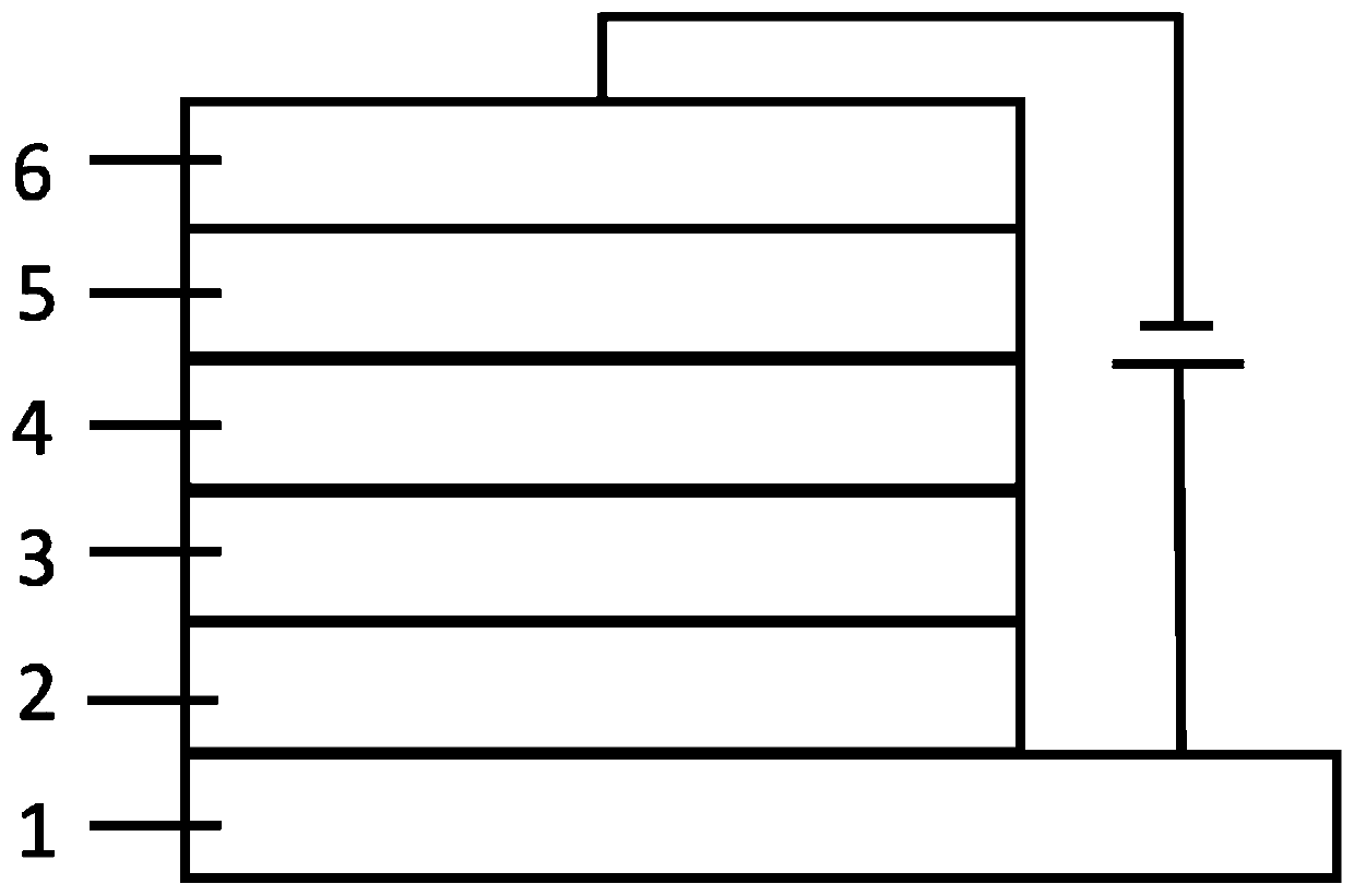
[0073] C) sequentially evaporating an electron transport layer, a cathode modification layer and a metal electrode on the surface of the perovskite layer to obtain a light emitting diode.
[0074] The present invention first carries out pretreatment to conductive glass substrate, and concrete method is as follows:
[0075] The patterned ITO or FTO conductive glass was ...
Embodiment 1
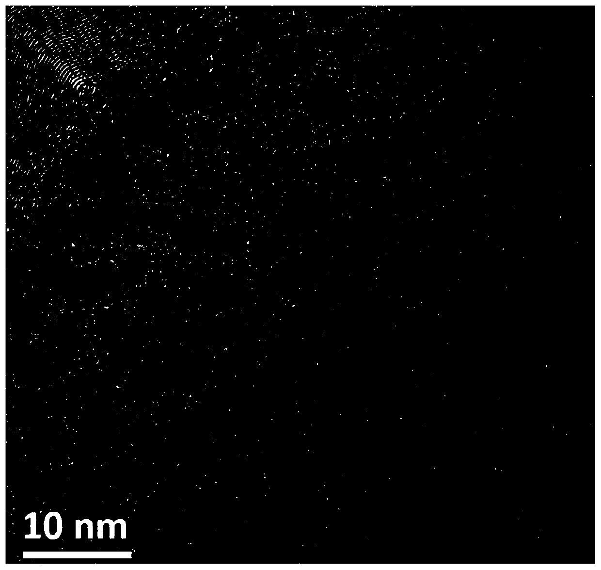
[0084] Dissolve 20 mg of 2,3-diaminonaphthalene and 50 mg of citric acid in 15 mL of ethanol solution, and sonicate for 10 minutes to promote its dissolution; transfer the completely dissolved clear solution to a 25 mL polytetrafluoroethylene reaction vessel, and Heating at 160°C for 4 hours; after the reaction was completed, the reactor was naturally cooled to room temperature; after that, the carbon quantum dots were purified by silica gel column chromatography using an appropriate proportion of dichloromethane and methanol as the eluent; The purified carbon quantum dots were dispersed in o-dichlorobenzene solvent to obtain a carbon quantum dot solution with a concentration of 10 mg / mL.
[0085] see figure 2 , figure 2 Transmission electron microscope picture of the carbon quantum dots prepared in Example 1. The particle size of the carbon quantum dots is 1.5-10 nm.
Embodiment 2
[0087] The preparation method of the perovskite light-emitting diode adopts the following steps:
[0088] (1) The patterned ITO conductive glass was ultrasonically cleaned with detergent, tap water, pure water, acetone and isopropanol for 15 minutes, and then dried with nitrogen gas and placed in an oven for drying. The dried conductive glass Carry out UV-ozone treatment for 15 minutes;
[0089] (2) Transfer the UV-ozone-treated conductive glass to a nitrogen glove box, place it on a homogenizer, spin-coat the carbon quantum dot solution prepared in Example 1 at 3000rpm for 30s, and then anneal at 80°C for 10min , so that the carbon quantum dot hole transport layer prepared on the conductive glass has a thickness of 30nm;
[0090] (3) Place the annealed substrate on a homogenizer, spin-coat the perovskite precursor solution at 4000rpm, and then anneal at 80°C for 10min to obtain a perovskite light-emitting layer with a thickness of 70nm. The perovskite precursor solution is ...
PUM
| Property | Measurement | Unit |
|---|---|---|
| Particle size | aaaaa | aaaaa |
| Thickness | aaaaa | aaaaa |
| Thickness | aaaaa | aaaaa |
Abstract
Description
Claims
Application Information
 - R&D
- Intellectual Property
- Life Sciences
- Materials
- Tech Scout
- Unparalleled Data Quality
- Higher Quality Content
- 60% Fewer Hallucinations
Browse by: Latest US Patents, China's latest patents, Technical Efficacy Thesaurus, Application Domain, Technology Topic, Popular Technical Reports.
© 2025 PatSnap. All rights reserved.Legal|Privacy policy|Modern Slavery Act Transparency Statement|Sitemap|About US| Contact US: help@patsnap.com