Trench type insulated gate bipolar transistor and preparation method thereof

A technology of bipolar transistors and insulated gates, which is applied in the field of trench-type insulated gate bipolar transistors and its preparation, can solve the deterioration of the trade-off relationship between conduction voltage drop and turn-off loss, increase the number of unbalanced carriers, and improve Turn-off loss and other issues, to achieve high critical breakdown field strength, improve conduction voltage drop and turn-off loss, and reduce turn-off loss

Active Publication Date: 2019-11-05
UNIV OF ELECTRONICS SCI & TECH OF CHINA
View PDF4 Cites 2 Cited by
  • Summary
  • Abstract
  • Description
  • Claims
  • Application Information

AI Technical Summary

Problems solved by technology

[0002] figure 1 It shows a semi-cellular structure of a traditional trench type all-silicon-based IGBT device. Although the IGBT has a conductance modulation effect, which reduces the forward conduction voltage drop to a certain extent, in order to achieve a higher withstand voltage, it must not The thickness of the drift region is not increased, but this increases the conduction voltage drop. Therefore, it is necessary to increase the back injection efficiency to reduce the conduction voltage drop. The increase in injection efficiency causes the unbalanced carrier extraction during the turn-off process. The number increases, thereby increasing the turn-off time, increasing the turn-off loss, and deteriorating the trade-off relationship between the conduction voltage drop and the turn-off loss

Method used


Image

  • Trench type insulated gate bipolar transistor and preparation method thereof
  • Trench type insulated gate bipolar transistor and preparation method thereof
  • Trench type insulated gate bipolar transistor and preparation method thereof

Examples


Embodiment Construction

[0054] The principles and features of the present invention are described below in conjunction with the accompanying drawings, and the examples given are only used to explain the present invention, and are not intended to limit the scope of the present invention.

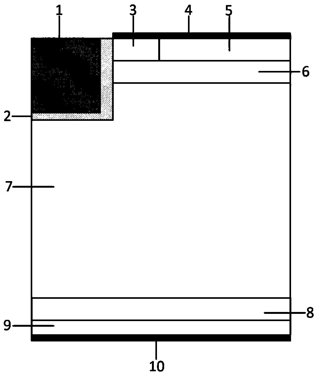
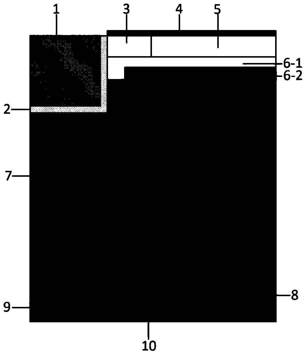
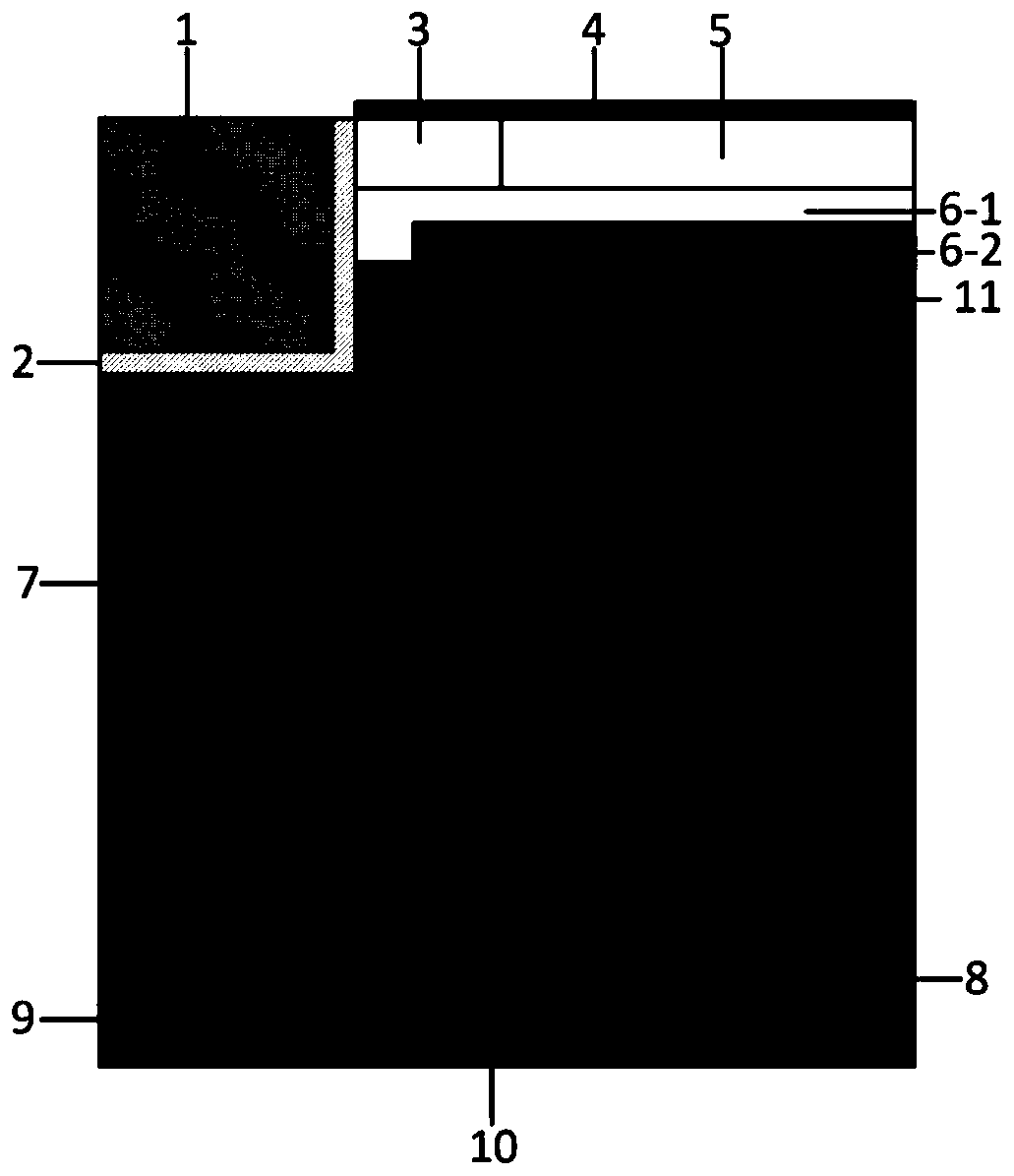
[0055] Considering that silicon-based devices have higher channel mobility, lower channel resistance, and lower interface state density than wide-bandgap semiconductor materials such as silicon carbide, and wide-bandgap materials such as silicon carbide have a large bandgap width. , its critical breakdown electric field is high, and under the same structure size, its breakdown voltage is much higher than that of silicon materials, so if under the same breakdown voltage, the thickness of the drift region of silicon carbide devices can be smaller, thereby reducing The conduction voltage drop is improved, and the trade-off relationship between the conduction voltage drop and the turn-off loss is improved. Therefore, in...


PUM


Abstract

The invention provides a trench type insulated gate bipolar transistor and a preparation method thereof, which belong to the technical field of power semiconductors. According to the invention, a narrow bandgap semiconductor material is used to form a conductive channel and form ohmic contact with emitter metal due to the characteristics of high channel mobility of a narrow bandgap material such as silicon and small ohmic contact resistance with the emitter metal; channel resistance and ohmic resistance are reduced; the forward conduction voltage drop of a device is reduced; in addition, due to the characteristic of high critical breakdown field strength of a wide bandgap material such as silicon carbide, the device is not limited by a gate oxide layer and prevented from avalanche breakdown; the position of a breakdown point is changed; the breakdown voltage of the device is improved to a certain extent, so that the thickness of a drift region can be appropriately reduced at a certainvoltage level; the forward conduction voltage drop and the turn-off loss are further reduced; and the trade-off relationship between the turn-on voltage drop and the turn-off loss is optimized. In addition, the invention further provides a preparation method of the trench type insulated gate bipolar transistor.

Description

technical field [0001] The invention belongs to the technical field of power semiconductors, and in particular relates to a trench type insulated gate bipolar transistor and a preparation method thereof. Background technique [0002] figure 1 It shows a semi-cellular structure of a traditional trench type all-silicon-based IGBT device. Although the IGBT has a conductance modulation effect, which reduces the forward conduction voltage drop to a certain extent, in order to achieve a higher withstand voltage, it must not The thickness of the drift region is not increased, but this increases the conduction voltage drop. Therefore, it is necessary to increase the back injection efficiency to reduce the conduction voltage drop. The increase in injection efficiency causes the unbalanced carrier extraction during the turn-off process. The number increases, thereby increasing the turn-off time, increasing the turn-off loss, and deteriorating the trade-off relationship between the co...

Claims


Application Information

Patent Timeline
Patent Type & Authority Applications(China)
IPC IPC(8): H01L29/739H01L29/267H01L21/331
CPCH01L29/267H01L29/66348H01L29/7397
Inventor 张金平罗君轶陈子珣刘竞秀李泽宏张波
Owner UNIV OF ELECTRONICS SCI & TECH OF CHINA
Why Eureka
Try Eureka