Graphene / doped two-dimensional layered material Van der Waals heterojunction superconducting composite structure, superconducting device and manufacturing method thereof

A two-dimensional layered, graphene layer technology, applied in the direction of devices containing a node of different materials, superconductive devices, superconductor parts, etc., can solve the problem of large non-zero effective mass of carriers, superconducting transition Low temperature and other problems, to achieve the effects of good mechanical properties and machining properties, low material cost, and simple structure

Active Publication Date: 2019-11-08
孙旭阳
View PDF22 Cites 5 Cited by
  • Summary
  • Abstract
  • Description
  • Claims
  • Application Information

AI Technical Summary

Problems solved by technology

However, because the bandgap that can be opened by the above method is too small, the Fermi level shifts too little, the available superconducting transition temperature is relatively low, and intercalation, doping and other means destroy the ideal crystal structure of graphene, making the loading Fluors acquire a large non-zero effective mass and no longer have the Dirac fermion properties of lossless ballistic transport

Method used


Image

  • Graphene / doped two-dimensional layered material Van der Waals heterojunction superconducting composite structure, superconducting device and manufacturing method thereof

Examples


preparation example Construction

[0053] According to a third aspect of the present invention, a method for preparing the above-mentioned superconducting device is provided. The upper and lower layers are graphene, and the middle is a "sandwich" structure of a doped two-dimensional layered material as an example, including the following step:

[0054] With the aid of the supporting compression block, place the first graphene layer first, transfer the doped two-dimensional layered material on the first graphene layer, and then transfer the second graphene layer on the doped two-dimensional layered material on the graphene layer, and press it with two pairs of supporting compression blocks arranged at intervals; two pairs of upper and lower metal electrodes are respectively arranged on the first and second graphene layers, and after alignment, the tabs are welded to form positive and negative electrodes, and a superconducting device is obtained.

[0055] The preparation method of a typical "sandwich" structure s...

Embodiment 1

[0060] Monolayer graphene / p-doped monolayer hexagonal boron nitride (h-BN) / monolayer graphene van der Waals heterojunction structure. The uppermost layer and the lower layer are all single-layer graphene, and the middle layer is p-doped single-layer hexagonal boron nitride (h-BN). Each layer is stacked into a "sandwich" structure in a van der Waals heterojunction manner.

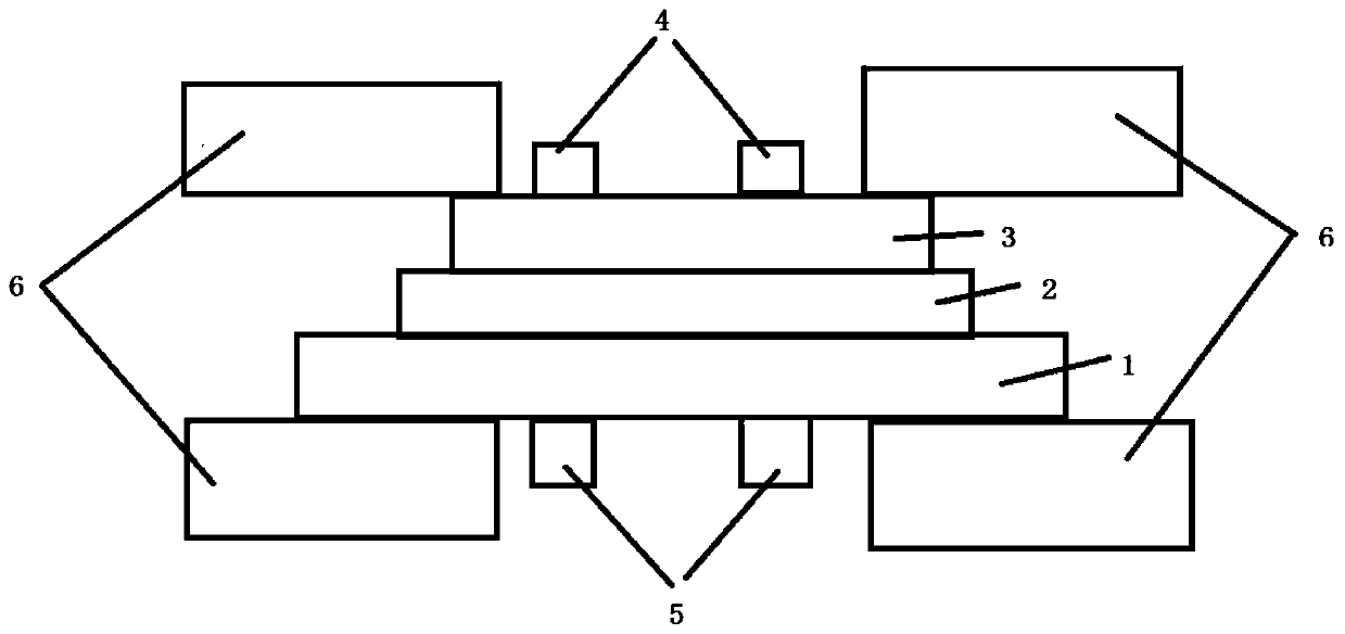
[0061] Among them, graphene was purchased from Nanjing Xianfeng Nano Material Technology Co., Ltd., p-doped single-layer hexagonal boron nitride was prepared by peeling off the corresponding bulk material repeatedly pasted with scotch tape, and p-doped by high-temperature diffusion method (doping concentration 1 to 10 -4 , at%). Such as figure 1 As shown, with the aid of an optical microscope, the above materials were stacked layer by layer. The length and width of the lowermost layer of graphene 1 are both 200 microns, the length and width of the middle single-layer hexagonal boron nitride 2 are about 10...

Embodiment 2

[0065] The difference between this embodiment and embodiment 1 is that the uppermost and lowermost layers are all single-layer graphene, and the middle layer is n-doped few-layer molybdenum disulfide (MoS 2 ), each layer self-assembles into a "sandwich" structure in a van der Waals heterojunction manner.

[0066] Few-layer molybdenum disulfide was obtained by vapor-phase deposition on graphene substrates based on the decomposition of ammonium tetrathiomolybdate. The decomposition of ammonium tetrathiomolybdate is based on the following two reactions:

[0067] (1)(NH 4 ) 2 MoS 4 +H 2 →2NH 3 +H 2 S+MoS 3 ;

[0068] (2)MoS 3 →MoS 2 +S.

[0069] Wherein (1) formula reaction temperature is 500 ℃; (2) formula reaction temperature is about 950 ℃.

[0070]Place the suspended graphene (the electrode is below) that is pressed by two pairs of supporting compression blocks and has deposited metal electrodes in the tube furnace, and take measures to close the lower part so that...


PUM

PropertyMeasurementUnit
tensile strengthaaaaaaaaaa
superconducting critical temperatureaaaaaaaaaa

Abstract

The invention provides a graphene / doped two-dimensional layered material Van der Waals heterojunction superconducting composite structure, a superconducting device and a manufacturing method thereofand relates to the superconducting material technology field. A graphene layer and a layered structure of 2n + 1 layers formed by alternative doped two-dimensional layered materials are included. Anouter layer of the layered structure is the graphene layer, and the n is an integer of 1 to 50. A region where graphene and the doped two-dimensional layered material are completely overlapped vertically forms a superconducting region. The graphene layer and the doped two-dimensional layered material are self-assembled into one body by a Van der Waals force. A defect that an existing Van der Waalsheterojunction superconducting material can only work at an extremely low temperature is solved. The graphene / doped two-dimensional layered material heterojunction superconducting material has a simple structure, excellent performance, a high critical temperature and a high critical magnetic field, low material cost, and good mechanical and machining performance.

Description

technical field [0001] The invention relates to the technical field of superconducting materials, in particular to a graphene / doped two-dimensional layered material van der Waals heterojunction superconducting composite structure, a superconducting device and a preparation method thereof. Background technique [0002] Superconductivity refers to the property that the resistance of certain substances drops to zero under certain temperature conditions (generally lower temperatures). In 1911, Dutch physicist H. Kamaolin Onnes first discovered that mercury enters a superconducting state around 4.2K. In 1933, Meissner and Ossenfeld in the Netherlands jointly discovered that when the material is in a superconducting state, the magnetic induction in the superconductor is zero and has the so-called "Meissner effect" of diamagnetism. From 1986 to 1993, the record of critical superconducting temperature was raised to 138K by copper-oxygen materials, and a huge breakthrough was made i...

Claims


Application Information

Patent Timeline
Patent Type & Authority Applications(China)
IPC IPC(8): H01L39/12H01L39/02H01L39/22H01L39/24
CPCH10N60/80H10N60/85H10N60/128H10N60/01H10N60/10H10N60/12H10N60/0241
Inventor 孙旭阳
Owner 孙旭阳
Why Eureka
Try Eureka