Method and device for multi-line silicon chip cutting with free-solidified compound abrasives

A multi-wire cutting and composite abrasive technology, which is applied in grinding/polishing equipment, metal processing equipment, stone processing equipment, etc., can solve the problem of not meeting the development requirements of silicon wafers, making manufacturing technology more difficult, and affecting the effect of abrasives To achieve the effect of enhancing microscopic plastic cutting performance, reducing surface cracks, and reducing damage rate

Inactive Publication Date: 2019-11-26
HARBIN UNIV OF COMMERCE
View PDF6 Cites 2 Cited by
  • Summary
  • Abstract
  • Description
  • Claims
  • Application Information

AI Technical Summary

Problems solved by technology

The larger the silicon crystal ingot, the thinner the kerf, the longer and deeper the slit between the saw wire and the silicon crystal ingot, the more uneven the grinding fluid will be and even cut off, which will seriously affect the full play of the grinding fluid.
The development needs of the semiconductor silicon wafer industry have increasingly brought greater difficulty to manufacturing technology. The diameter of silicon wafers has gradually increased and the thickness has continued to decrease. The current processing methods cannot meet the development requirements of silicon wafers.

Method used


Image

  • Method and device for multi-line silicon chip cutting with free-solidified compound abrasives

Examples


Embodiment Construction

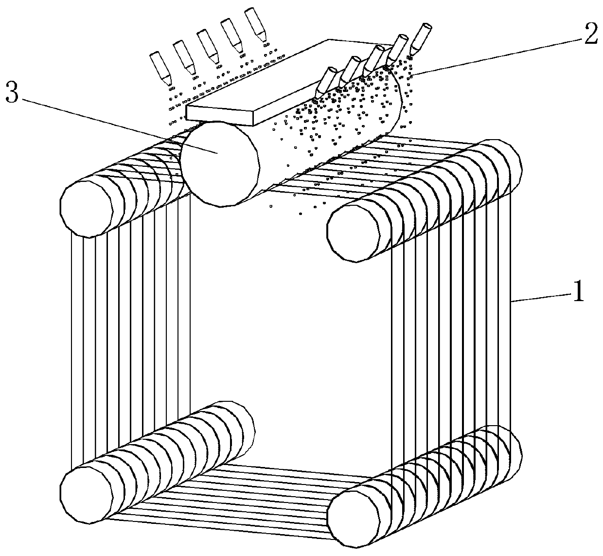
[0017] refer to figure 1 , a method for multi-wire cutting of silicon wafers with free-bonded composite abrasives, which includes sawing a silicon crystal ingot 3 by using a method of multi-wire cutting with fixed abrasives, and spraying the abrasive liquid 2 containing suspended diamond abrasive grains to the cutting area at the same time ; The metal wire 1 with diamond abrasive grains on the surface will bring the abrasive liquid 2 containing suspended diamond abrasive grains into the slit of the silicon ingot 3 during the wire walking process, forming free abrasive grains and consolidated abrasive grains to work together, The silicon crystal ingot 3 is sawed, and the silicon crystal ingot 3 is cut into several pieces in one process.

[0018] The free-bonded composite abrasive multi-wire cutting device for silicon wafers includes free abrasive multi-wire cutting equipment, and diamond abrasive grains are consolidated on the surface of all metal wires 1 of the free abrasive m...


PUM

PropertyMeasurementUnit
Diameteraaaaaaaaaa
The average particle sizeaaaaaaaaaa

Abstract

A method and device for multi-line silicon chip cutting with free-solidified compound abrasives belong to the technical field of processing of semiconductor materials and solve problems in silicon crystal slicing. The method for multi-line silicon chip cutting with the free-solidified compound abrasives comprises the steps that a silicon crystal ingot is cut through multi-line cutting with solidified abrasives, and a grinding solution containing suspended diamond abrasive granules is sprinkled to a cut area; and a metal wire with the diamond abrasive particles solidified on the surface bringsthe grinding solution containing the suspended diamond grinding particles into a cutting seam of the silicon crystal ingot during wire walking, so joint effects of free abrasives and the solidified abrasives are formed to jointly cut the silicon crystal ingot, and the silicon crystal ingot is cut into multiple slices during one time of processing. The device for multi-line silicon chip cutting with the free-solidified compound abrasives comprises a free abrasive multi-line cutting device, wherein the diamond abrasive particles are solidified on surfaces of all the metal wires of the free abrasive multi-line cutting device. The method and device provided by the invention are applied to cutting of silicon chips.

Description

technical field [0001] The invention belongs to the technical field of semiconductor material processing, and in particular relates to a method and equipment for multi-wire cutting of silicon wafers with free-solidified composite abrasives. Background technique [0002] Silicon-based semiconductor processing technology is a key technical condition for the development of high-tech industries such as integrated circuits, electronic information, and solar photovoltaics. Silicon crystal slicing is the front-end process of the semiconductor processing industry chain, and its processing capacity directly determines the performance and quality of subsequent processes and end products. In order to continuously improve the performance and economic benefits of end products, silicon crystal slicing processing technology is required to develop in the direction of large diameter, small thickness, high quality, high production capacity, high efficiency and low consumption. In the process...

Claims


Application Information

Patent Timeline
IPC IPC(8): B28D5/04B28D7/00B24B27/00B24B27/06B24B57/04
CPCB24B27/0076B24B27/0633B24B57/04B28D5/007B28D5/045
Inventor 冯砚博陈博高博文
Owner HARBIN UNIV OF COMMERCE
Why Eureka
Try Eureka