Communication chip and preparation method for homogenously integrated light source, detector and active waveguide

A communication chip and detector technology, which is applied in semiconductor/solid-state device manufacturing, semiconductor devices, electric solid-state devices, etc., can solve the complex preparation process of heterogeneous integrated communication chip devices, the insulating isolation layer cannot provide effective light reflection, passive The problem of large waveguide transmission loss, etc., can improve the success rate of preparation, realize wafer-level integration, and reduce the difficulty of preparation.

Active Publication Date: 2021-09-28
NANJING INST OF TECH
View PDF10 Cites 0 Cited by
  • Summary
  • Abstract
  • Description
  • Claims
  • Application Information

AI Technical Summary

Problems solved by technology

[0005] Technical purpose: The technical problem to be solved by the present invention is to provide a communication chip and a preparation method for homogenously integrated light sources, detectors and active waveguides, which can solve the problem of complex preparation process of heterogeneous integrated communication chip devices, which cannot be integrated at the wafer level. Problem, the present invention uses the active waveguide to provide stable optical energy gain when transmitting optical signals, and can solve the problems of large transmission loss and insufficient transmission distance of the traditional gallium nitride passive waveguide; the dielectric Bragg reflector is used as an insulating isolation layer, Can solve traditional SiO 2 The insulating isolation layer cannot provide effective light reflection, which is not conducive to the problem of confining outgoing photons inside the device

Method used


Image

  • Communication chip and preparation method for homogenously integrated light source, detector and active waveguide
  • Communication chip and preparation method for homogenously integrated light source, detector and active waveguide
  • Communication chip and preparation method for homogenously integrated light source, detector and active waveguide

Examples


Embodiment Construction

[0032] The following examples further illustrate the content of the present invention, but should not be construed as limiting the present invention. Without departing from the spirit and essence of the present invention, the modifications and substitutions made to the methods, steps or conditions of the present invention all belong to the scope of the present invention.

[0033] Example:

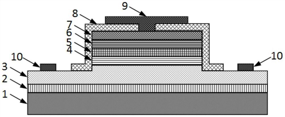
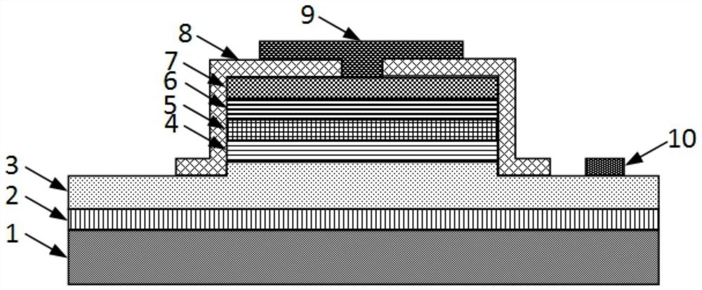
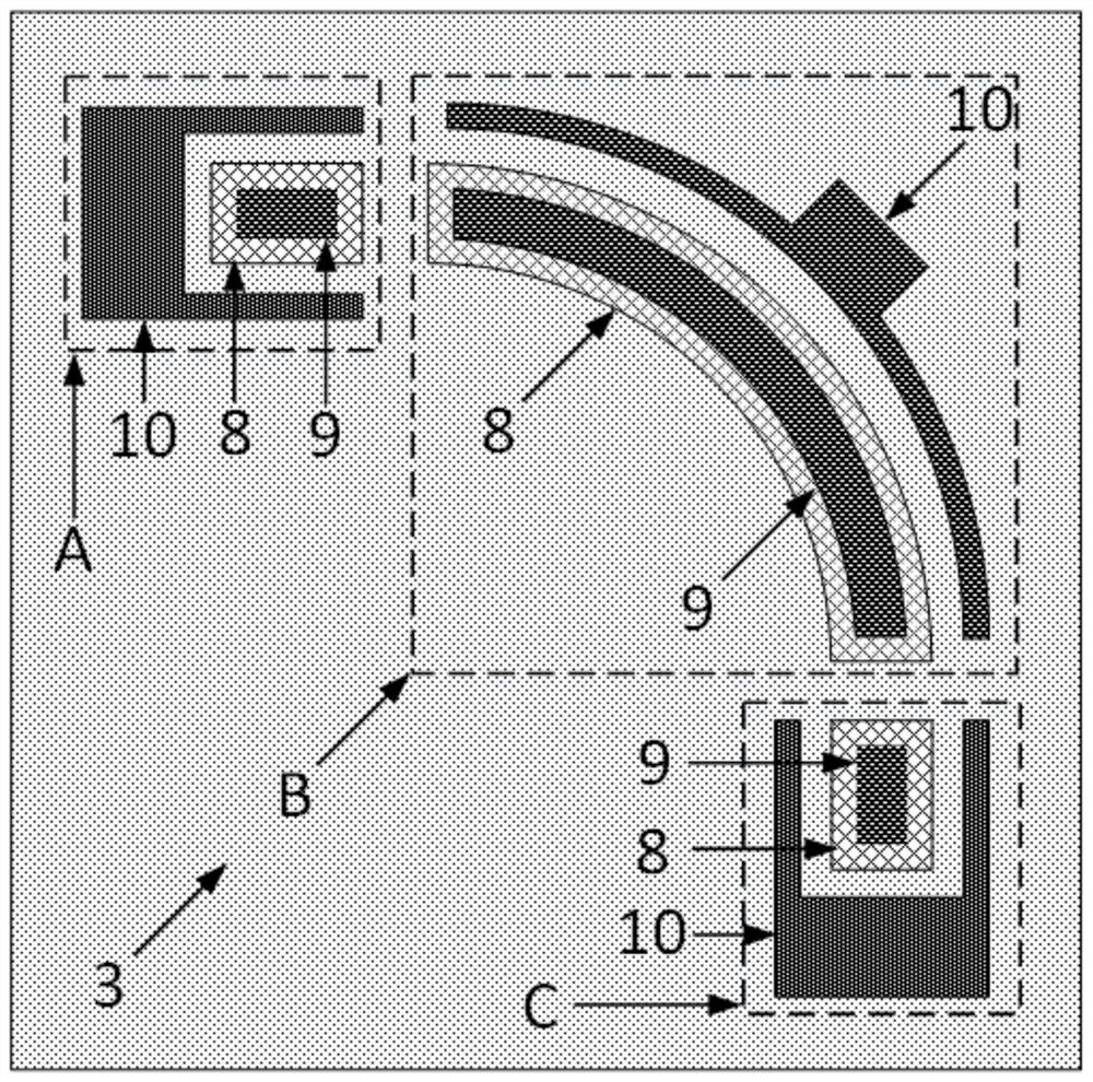
[0034] like figure 1 , figure 2 , image 3 and Figure 4 As shown, a communication chip with a homogenously integrated light source, detector and active waveguide is prepared based on a GaN wafer on a silicon substrate, and the GaN wafer on a silicon substrate includes a p-GaN layer from top to bottom 7. InGaN multi-quantum well layer 6, InGaN waveguide layer 5, AlGaN cladding layer 4, n-GaN layer 3, buffer layer 2 and silicon substrate layer 1. The communication chip that homogeneously integrates light source, detector and active waveguide is prepared based on silicon substrate gallium...


PUM

PropertyMeasurementUnit
thicknessaaaaaaaaaa
thicknessaaaaaaaaaa
thicknessaaaaaaaaaa

Abstract

The invention discloses a communication chip with a homogenous integrated light source, a detector and an active waveguide and a preparation method. The communication chip is prepared based on a silicon substrate gallium nitride wafer, and the silicon substrate gallium nitride wafer is from top to bottom The bottom layer sequentially includes a p-GaN layer, an InGaN multiple quantum well layer, an InGaN waveguide layer, an AlGaN cladding layer, an n-GaN layer, a buffer layer and a silicon substrate layer, and a light source, a detector and an active waveguide are arranged on the buffer layer. The light source, detector and active waveguide all include p-n junctions, insulating isolation layers, p-type electrodes and n-type electrodes, and each p-n junction is formed by etching the silicon substrate gallium nitride wafer. The invention can solve the problems of complex preparation process of heterogeneous integrated communication chip devices and cannot be integrated at wafer level, simplifies the preparation process, has low transmission loss, can be applied to the fields of optical communication and optical sensing, and can realize longer-distance on-chip optical signals transmission.

Description

technical field [0001] The invention relates to the field of information materials and devices, in particular to a communication chip and a preparation method for homogeneously integrating a light source, a detector and an active waveguide. Background technique [0002] The application research of Gallium Nitride material is the frontier and hotspot of global semiconductor research at present. It is a new type of semiconductor material for the development of microelectronic devices and optoelectronic devices. The third generation of semiconductor materials after semiconductor materials. Gallium nitride material has wide direct bandgap, strong atomic bond, high thermal conductivity, good chemical stability, strong radiation resistance, and has triple functions of light emission, light transmission and light detection. Devices have extremely broad application prospects, providing a physical basis for the development of homogeneous integrated communication chips. [0003] At ...

Claims


Application Information

Patent Timeline
Patent Type & Authority Patents(China)
IPC IPC(8): H01L27/15H01L33/00H01L33/44H01L33/46H01L21/8252
CPCH01L21/8252H01L27/15H01L33/0066H01L33/0075H01L33/44H01L33/46H01L2933/0025
Inventor 蔡玮韩冰王新迪
Owner NANJING INST OF TECH
Why Eureka
Try Eureka