

Low-power-consumption and high-reliability trench silicon carbide MOSFET device
A reliable, trench-type technology, applied to semiconductor devices, electrical components, circuits, etc., can solve problems such as weak short-circuit capability, high switching loss, and large gate-to-drain capacitance, so as to reduce saturation current, improve short-circuit capability, and reduce The Effect of Switching Losses
- Summary
- Abstract
- Description
- Claims
- Application Information
AI Technical Summary
Problems solved by technology
Method used
Image

Examples
Embodiment 1
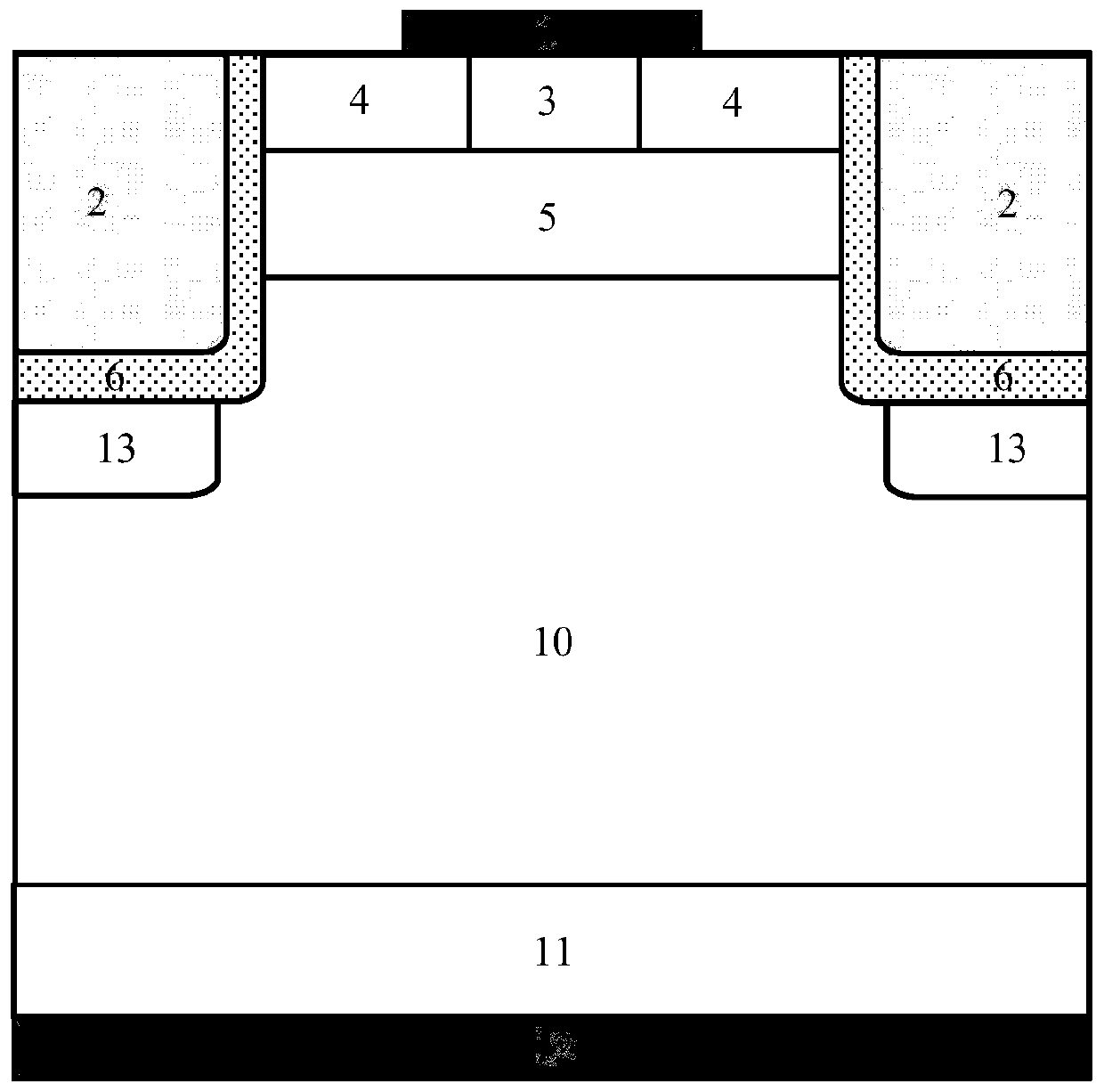
[0026] Such as figure 2 As shown, a trench silicon carbide MOSFET device with low power consumption and high reliability of this embodiment includes: an N-type substrate 11, an N-type epitaxial layer 10 located above the N-type substrate 11, and an N-type epitaxial layer The second P-body area 9 above the layer 10, the second P+ contact area 7 and the second N+ contact area 8 located inside the second P-body area 9, the second P+ contact area 7 and the second N+ contact area 8 The upper source electrode 1, the gate dielectric 6 located above the second N+ contact region 8, and the trench gate inside the gate dielectric 6, the first P-body region 5 located between the gate dielectrics 6, and the first P-body region 5 the two first N+ contact regions 4 above, the first P+ contact region 3 between the two first N+ contact regions 4, the source electrode 1 located above the first P+ contact region 3 and the first N+ contact region 4 The drain electrode 12 is located under the devi...
Embodiment 2
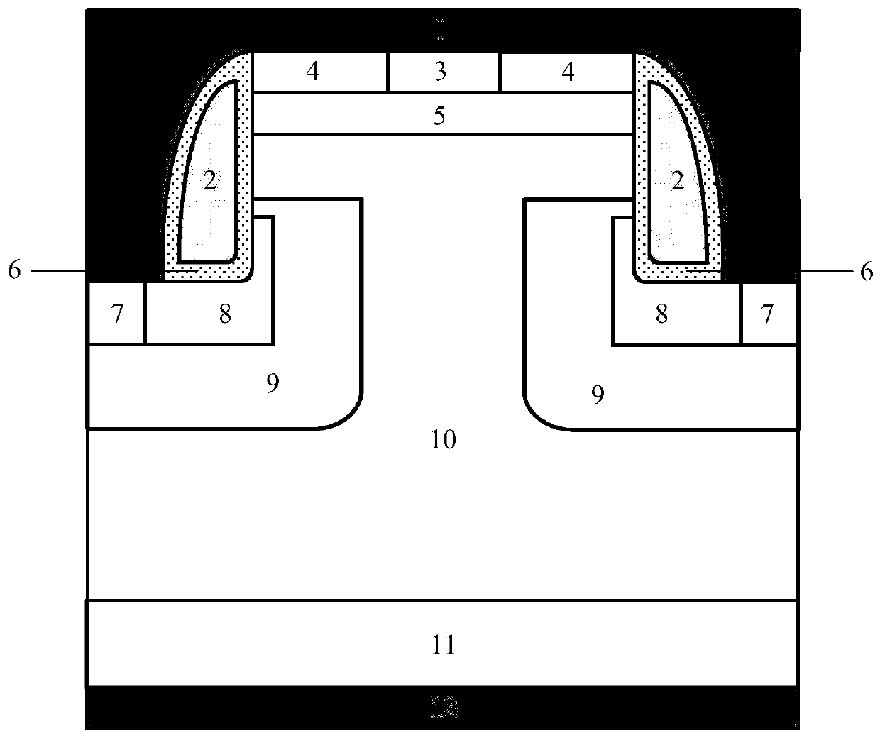
[0030] Such as image 3 As shown, the difference between the device structure of this embodiment and Embodiment 1 is that the trench gate 2 and the gate dielectric 6 are in an inverted L shape, and the inverted L shape includes a horizontal section and a vertical section connected below the horizontal section. An N-type epitaxial layer 10 is provided between a P-body region 5 and the gate dielectrics 6 on both sides. The horizontal sections of the trench gate 2 and the gate dielectric 6 are located in the first N+ contact region 4, the first P-body region 5 and N Above the type epitaxial layer 10, a gate dielectric 6 is provided between the trench gate 2 and the first N+ contact area 4, the first P-body area 5, and the N type epitaxial layer 10.
Embodiment 3
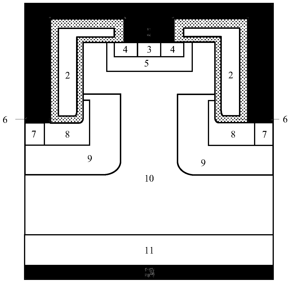
[0032] Such as Figure 4 As shown, two first P-body regions 5 are provided between the gate dielectric 6, two first P+ contact regions 3 are provided between the two first N+ contact regions 4, and one of the two first P+ contact regions 3 An N-type epitaxial layer 10 is provided between and between the two first P-body regions 5, and the N-type epitaxial layer 10 forms a Schottky contact with the source electrode 1. The advantage of this is that the performance of the third quadrant of the device is improved.
PUM
 Abstract
Description
Claims
Application Information