Ceramic circuit board, method for manufacturing ceramic circuit board, and module using ceramic circuit board

A technology for circuit substrates and ceramic substrates, applied in circuits, printed circuits, electrical components, etc., can solve the problems of weak solder layer and reduced thermal cycle characteristics, and achieve the effect of excellent thermal cycle characteristics and good productivity

Pending Publication Date: 2019-12-03
DENKA CO LTD
View PDF6 Cites 1 Cited by
  • Summary
  • Abstract
  • Description
  • Claims
  • Application Information

AI Technical Summary

Problems solved by technology

[0006] In Patent Document 2, jointing at a temperature of 750° C. to 850° C. is studied under a nitrogen atmosphere using solder containing zirconium. However, there is a problem that the solder layer is deformed due to the influence of zirconium added in a large amount to ensure jointability. Fragile, reduced heat cycle resistance

Method used


Image

  • Ceramic circuit board, method for manufacturing ceramic circuit board, and module using ceramic circuit board
  • Ceramic circuit board, method for manufacturing ceramic circuit board, and module using ceramic circuit board
  • Ceramic circuit board, method for manufacturing ceramic circuit board, and module using ceramic circuit board

Examples


Embodiment 1

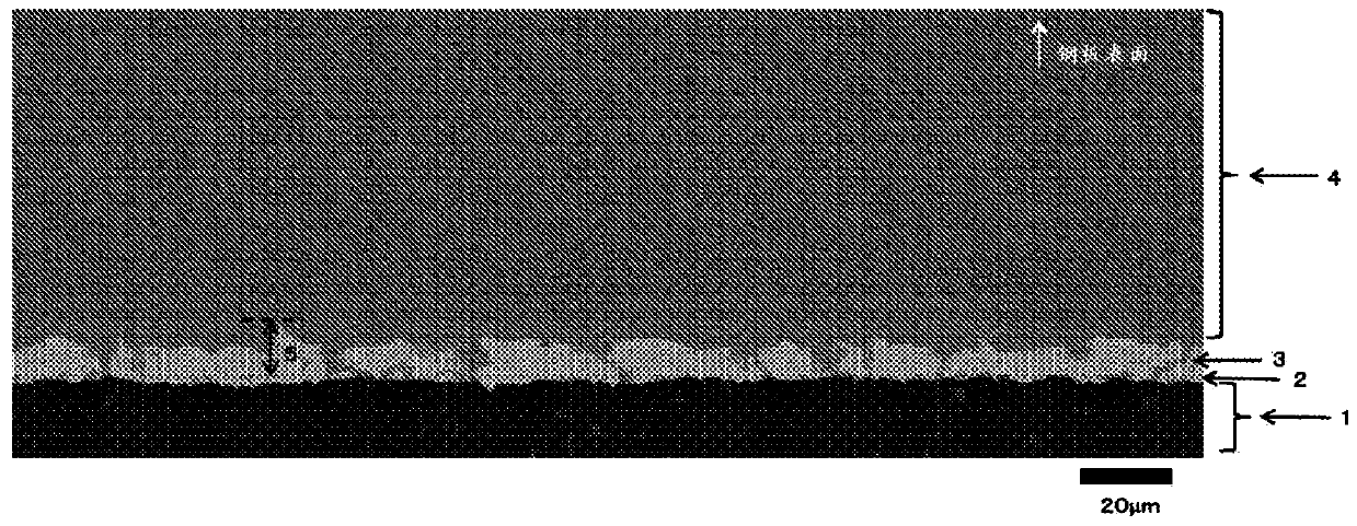
[0051] Using a roll coater, 88 parts by mass of Ag powder ("AgC-BO" manufactured by Fukuda Metal Foil Powder Industry Co., Ltd.) and 12 parts by mass of Cu powder ("SRC-Cu" manufactured by Fukuda Metal Foil Powder Industry Co., Ltd.) -20 ") of a total of 100 parts by mass of the mixture and mix 2.5 parts by mass of TiH 2 powder ("TSH-350" manufactured by Osaka Titanium Technology Co., Ltd.), 4 parts by mass of Sn powder ("Sn powder (-325 mesh)" manufactured by Mitsuwa Pharmaceutical Chemical Co., Ltd.), and the solder paste thus formed was prepared by 8mg / cm 2 The amount of coating is applied to a silicon nitride substrate with a thickness of 0.32mm. Then, a copper plate for forming a circuit was overlaid on one side of the silicon nitride substrate, and a copper plate for forming a heat dissipation plate (both oxygen-free copper plates with a thickness of 0.8 mm) was overlaid on the other side of the silicon nitride substrate, and they were put into a nitrogen atmosphere. T...

Embodiment 2~7、 comparative example 2~10

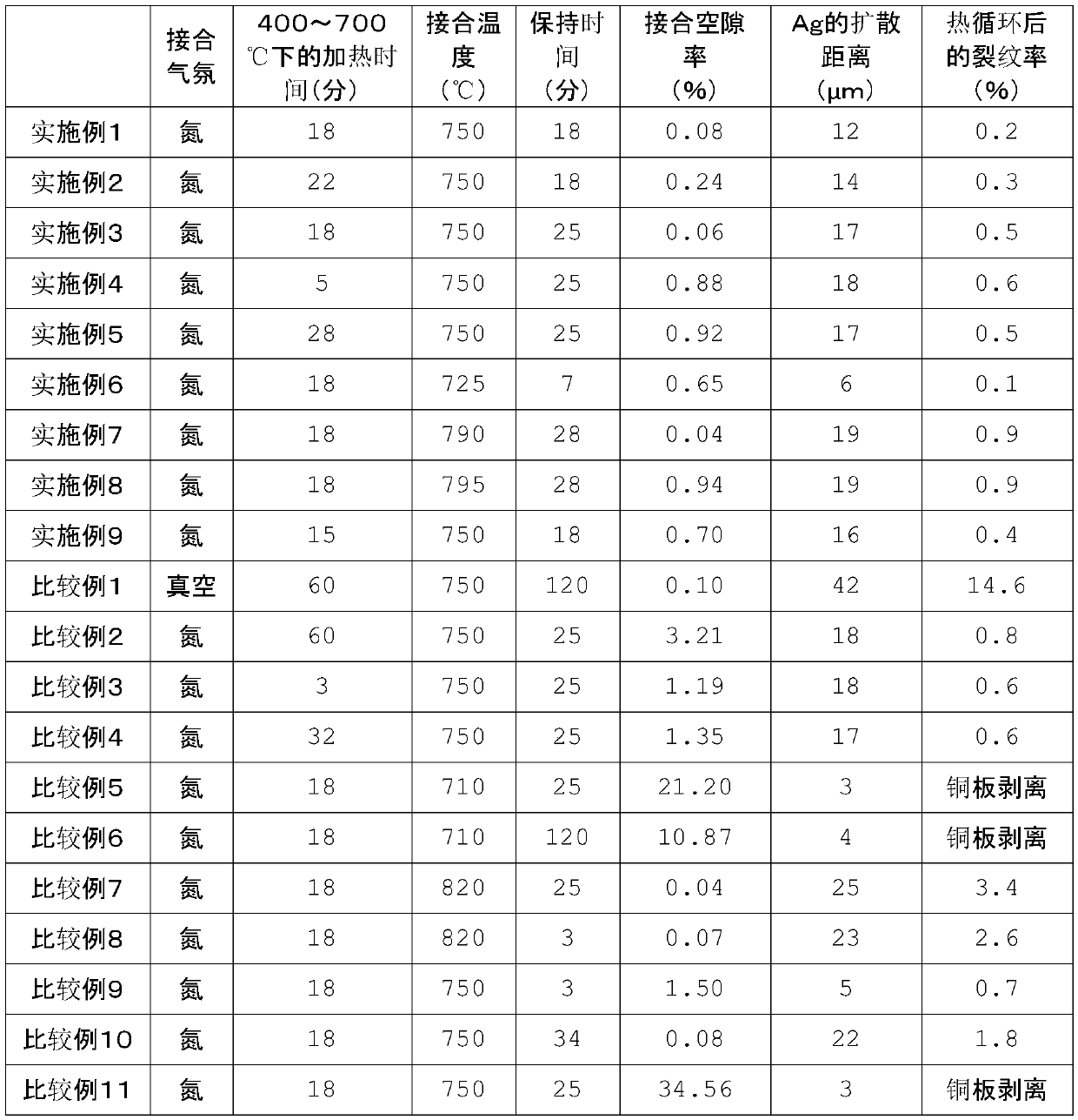
[0057] Ceramic circuit boards were obtained in the same manner as in Example 1 except that the bonding atmosphere, the heating time in the temperature range of 400° C. to 700° C., the bonding temperature, and the holding time were changed as shown in Table 1. Table 1 shows the measurement results.

Embodiment 8

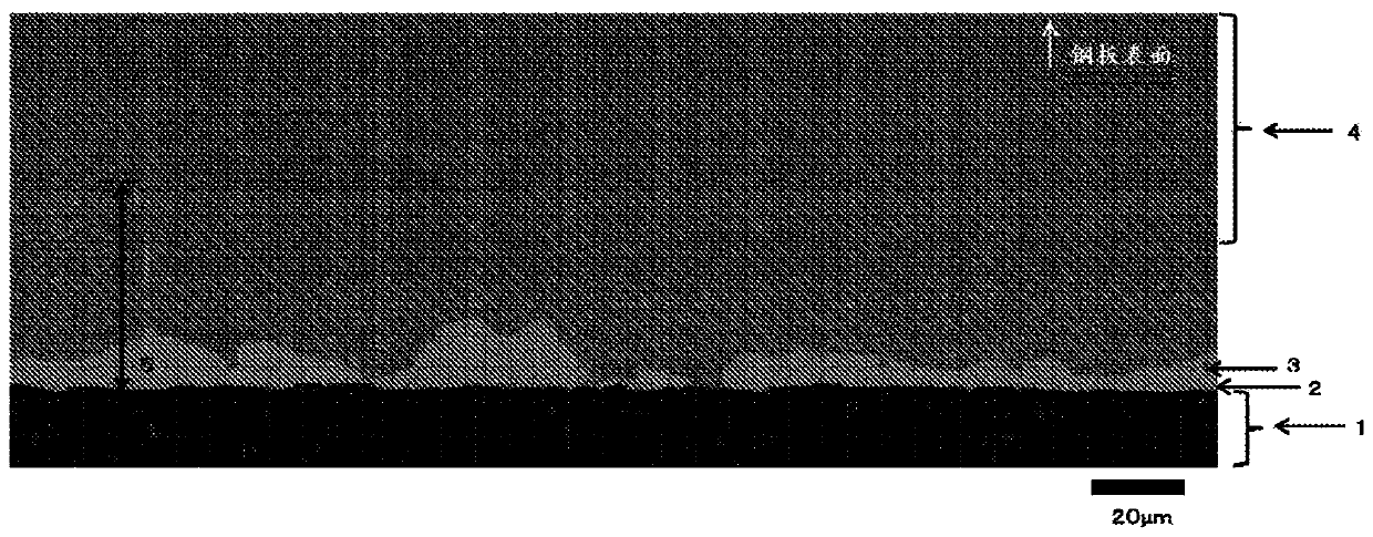
[0059] A ceramic circuit board was obtained in the same manner as in Example 1 except that no Sn powder was added and the bonding temperature and holding time were changed as shown in Table 1. Table 1 shows the measurement results.


PUM

PropertyMeasurementUnit
Thicknessaaaaaaaaaa

Abstract

The present invention provides a ceramic circuit board and a power module with outstanding heat resistance cycle properties. Provided is a ceramic circuit board, formed by a ceramic substrate and a copper plate being bonded via a brazing filler material that contains silver, copper, and an active metal, wherein the bonding void ratio is 1.0% or less and the diffusion distance of the silver as a constituent of the brazing filler material is 5-20 [mu]m. Also provided is a method for manufacturing the ceramic circuit board, characterized in that: the heating time in the 400-700 DEG C temperaturerange during a step in which the temperature is raised to a bonding temperature is 5-30 minutes; and bonding is performed by maintaining a bonding temperature of 720-800 DEG C for 5-30 minutes.

Description

technical field [0001] The present invention relates to a ceramic circuit board, a manufacturing method thereof, and a component using the ceramic circuit board. Background technique [0002] Ceramic circuit boards, in which metal circuit boards, metal heat sinks, and ceramic substrate surfaces are bonded, are used in power modules for electric railways, vehicles, and industrial machinery that require high-voltage, high-current operation. In recent years, with the high output power and high integration of semiconductor elements, the heat generation of semiconductor elements has been increasing. In order to efficiently release the generated heat, silicon nitride sintered bodies with high thermal conductivity, Ceramic substrate composed of aluminum nitride sintered body. [0003] In particular, higher heat dissipation is required for automotive power modules, and research has been conducted on thinner ceramic substrates and thicker metal plates. However, if such a structure ...

Claims


Application Information

Patent Timeline
IPC IPC(8): H01L23/36H01L23/12H01L25/07H01L25/18
CPCH01L23/12H01L23/36H01L25/07H01L25/18C04B2237/60C04B2237/124C04B2237/125C04B2237/126C04B2237/366C04B2237/368C04B37/026C04B2235/77C04B2235/6562C04B2237/708C04B2235/6567C04B2235/658H01L23/15H01L23/3735H01L23/3736C04B2237/407H05K1/0306
Inventor 原田祐作汤浅晃正中村贵裕森田周平西村浩二
Owner DENKA CO LTD
Why Eureka
Try Eureka