Method for preparing graphene and graphene device by epitaxy of pretreated SiC substrate

A graphene and pretreatment technology, applied in the field of microelectronic materials, can solve the problems of reduced growth rate, random microscopic nucleation sites, etc., and achieve the effects of reducing nucleation density, high-quality surface morphology, and high safety factor

Active Publication Date: 2019-12-10
SHANDONG UNIV
View PDF9 Cites 2 Cited by
  • Summary
  • Abstract
  • Description
  • Claims
  • Application Information

AI Technical Summary

Problems solved by technology

However, in the above process, the growth rate is only reduced on the macroscopi

Method used


Image

  • Method for preparing graphene and graphene device by epitaxy of pretreated SiC substrate
  • Method for preparing graphene and graphene device by epitaxy of pretreated SiC substrate
  • Method for preparing graphene and graphene device by epitaxy of pretreated SiC substrate

Examples


Embodiment 1

[0051] A method for preparing graphene and graphene devices by pretreatment of SiC substrate epitaxy, comprising steps as follows:

[0052] (1) Hydrogen etching

[0053] The SiC wafer obtained by cutting, grinding, mechanical polishing and chemical mechanical polishing of the SiC block has regular atomic-level steps on the surface, and is then cleaned by RCA standard cleaning method. Introduce hydrogen gas into the furnace cavity for hydrogen etching. The hydrogen etching temperature is 1600°C, the hydrogen flow rate is 50 sccm, the argon gas flow rate is 800 sccm, the pressure is 900 mbar, and the hydrogen etching time is 30 minutes; after that, vacuuming is performed, and the vacuum degree is 5×10 -5 Pa; completely pump out the gas in the furnace chamber;

[0054] (2) oxidation

[0055] Perform pre-oxidation treatment on the wafer after hydrogen etching, the oxygen flow rate is 20 sccm, the argon gas flow rate is 800 sccm, the chamber pressure is 800 mbar, the temperature ...

Embodiment 2

[0061] A method for preparing graphene and graphene devices by pretreatment of SiC substrate epitaxy, comprising steps as follows:

[0062] As described in Example 1, the difference is that the growth surface used is the (000-1) carbon surface of SiC, the SiC wafer is placed in the furnace chamber, and then the oxidation treatment process is carried out, the oxidation temperature is 500°C, and the oxygen flow rate 50sccm, oxidation treatment time 60min; graphene growth temperature 1450°C, growth time 120min.

[0063] The epitaxially grown graphene wafer on the SiC substrate is subjected to metal evaporation, photolithography and integration procedures, and finally the corresponding MOSFET device is prepared, and the carrier mobility of the obtained SiC epitaxial graphene is ~10000cm 2 ·V -1 ·s -1 .

Embodiment 3

[0065] A method for preparing graphene and graphene devices by pretreatment of SiC substrate epitaxy, comprising steps as follows:

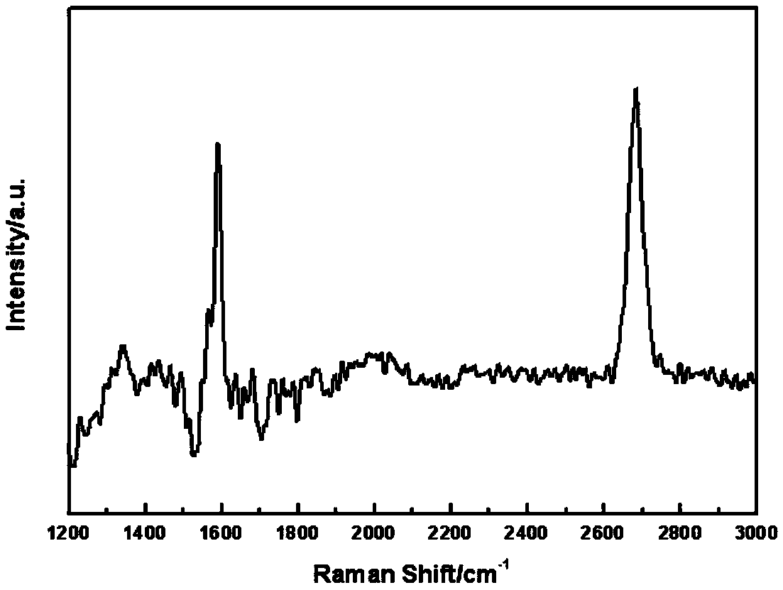
[0066] As described in Example 1, the differences are: oxidation temperature 1300°C, oxygen flow 5sccm, oxidation treatment time 120min; graphene growth temperature 1700°C, growth time 30min; temperature rise rate to reach the target growth temperature 5°C / min, During the cooling process, the cooling rate was 5°C / min. The number of layers of the grown graphene is uniform, and its morphology is as follows: Figure 5 shown.


PUM

PropertyMeasurementUnit
Thicknessaaaaaaaaaa

Abstract

The invention relates to a method for preparing graphene and a graphene device by epitaxy of a pretreated SiC substrate. The method comprises the following steps: performing hydrogen etching on the SiC substrate and then performing oxidation treatment on the SiC substrate after hydrogen etching at a temperature of 800-1300 DEG C for the treatment time of 15-120min; and then rising the temperatureto 1450-1700 DEG C in an inert atmosphere on the pretreated SiC substrate for graphene growth. The SiC surface is passivated through oxidation pretreatment so that nucleation density of the graphene epitaxially grown on the SiC substrate is reduced, the graphene material with larger size and better performance is obtained, and the SiC epitaxial graphene wafer is subjected to deposition, photolithography, doping and integration procedures accordingly so as to prepare the corresponding graphene device.

Description

technical field [0001] The invention relates to a method for preparing graphene and graphene devices by epitaxial pretreatment of SiC substrates, in particular to a method for epitaxially growing large crystal domains and high-quality graphene based on large-diameter 4H / 6H-SiC substrates, belonging to microelectronic materials technology field. Background technique [0002] Graphene is made of carbon atoms with sp 2 The atomic-level two-dimensional crystal material of the hexagonal honeycomb lattice formed by orbital hybridization has a high carrier mobility dozens of times that of commercial silicon wafers, and is little affected by temperature and doping effects, showing excellent Electron transport properties. Graphene crystals have important application value in ultra-high frequency electronic devices. However, the improvement of the performance of graphene electronic devices is severely restricted by the quality of graphene, and the preparation of high-quality, low-c...

Claims


Application Information

Patent Timeline
IPC IPC(8): H01L21/02
CPCH01L21/02378H01L21/02488H01L21/02527H01L21/02658
Inventor 孙丽于法鹏刘振兴李妍璐程秀凤陈秀芳赵显
Owner SHANDONG UNIV
Why Eureka
Try Eureka