
A mini LED light board, preparation method and display device

A technology of LED chips and light boards, applied in lighting devices, lighting device components, circuit layouts, etc., can solve problems such as solder joint breakage of MiniLED chips, reduce curing shrinkage, reduce curing stress, avoid displacement and The effect of solder joint fracture

Active Publication Date: 2022-07-08
HISENSE VISUAL TECH CO LTD
View PDF11 Cites 0 Cited by
  • Summary
  • Abstract
  • Description
  • Claims
  • Application Information

AI Technical Summary

Problems solved by technology

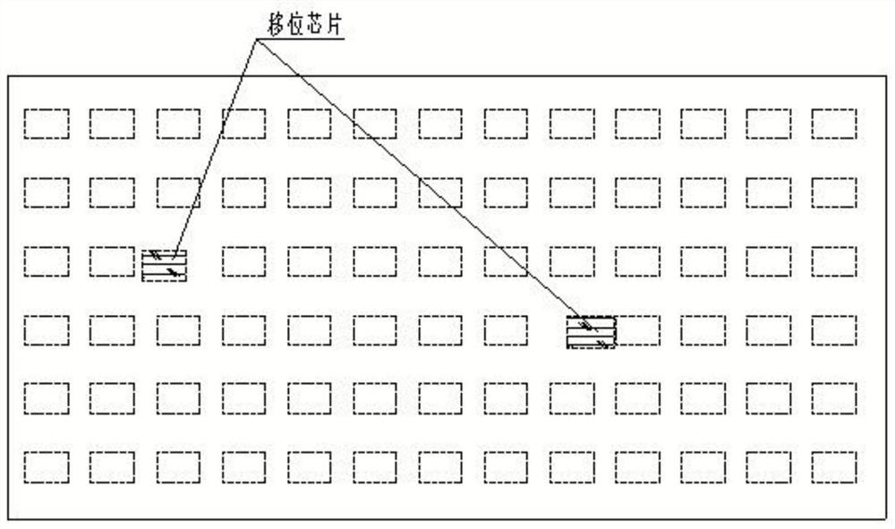
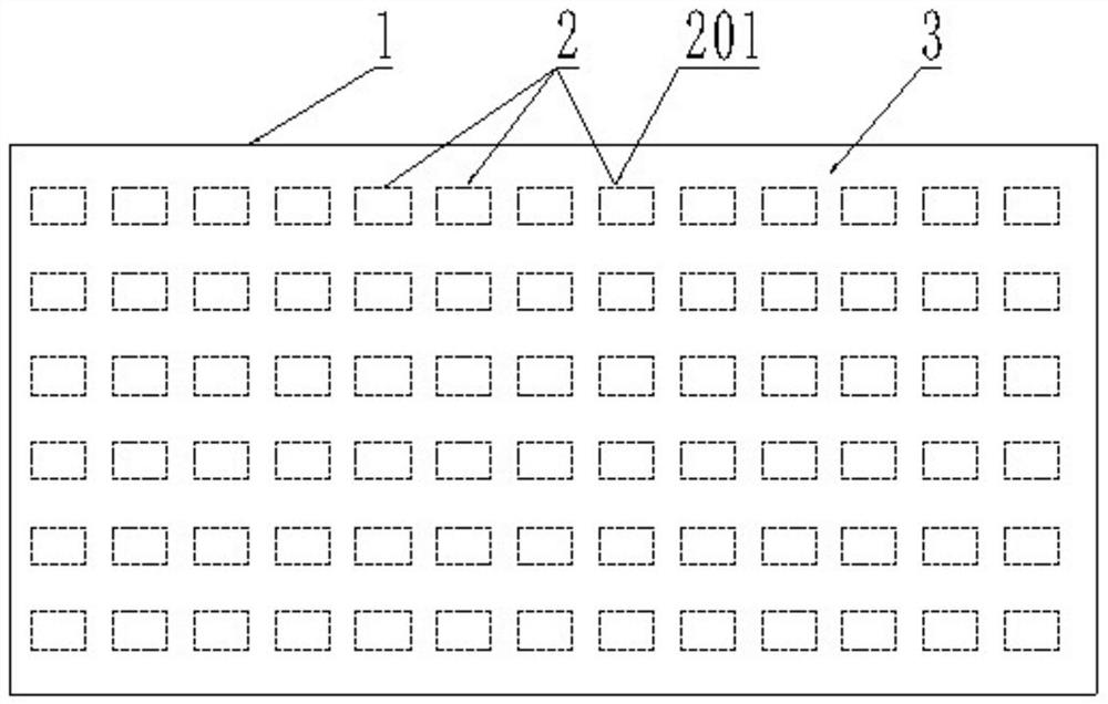
[0005] The application provides a Mini LED lamp board, a preparation method and a display device, which effectively solve the problems of displacement of the Mini LED chip and fracture of solder joints during the curing process of the packaging resin of the Mini LED lamp board, and improve the yield rate of the Mini LED lamp board

Method used


Image

  • A mini LED light board, preparation method and display device
  • A mini LED light board, preparation method and display device
  • A mini LED light board, preparation method and display device

Examples


preparation example Construction

[0049] The present application also provides a method for preparing a Mini LED light panel, as shown in the attached Figure 5 As shown, the method includes:

[0050] S101: Fixing the LED chip: fixing the LED chip to the circuit board to form a first LED chip board.

[0051] Obtain a circuit board, and fix the LED chip on the circuit board; usually, a chip fixing position is preset on the circuit board, such as setting a pad, and the LED chip is fixed according to the preset chip fixing position. Specifically, dispensing equipment is used to dispense silver paste point by point on the welding bracket of the circuit board, and a die bonding machine is used to transfer the LED chips to the welding bracket on the circuit board for fixed welding. Get the first LED chip board.

[0052] Among them, the LED chip can be obtained by cutting the LED wafer substrate by cutting technology. Usually, the LED chip on the substrate is cut by plasma, electron beam and other cutting technolog...

Embodiment 1

[0069] In a Mini LED light board, the composition ratio of the encapsulation layer is: bisphenol A epoxy resin 90g; nano-SiO 2 3g; silane coupling agent KH-570 0.1g; spirocyclic orthoester SOE expansion monomer 3g, curing agent chain flexible aromatic diamine 0.5g. The preparation of Mini LED light board is as follows:

[0070] Mix the silane coupling agent KH-570 into absolute ethanol, add glacial acetic acid, and configure it into an alcohol solution of silane coupling agent KH-570 with a pH value of 4. 2 Add the silane coupling agent KH-570 alcohol solution with the pH value of 4, electromagnetic stirring, ultrasonic dispersion and centrifugal treatment, grinding and drying to obtain modified nano-SiO 2 . The modified nano-SiO 2 , Expanding monomer and curing agent are added into epoxy acrylate, mixed at high speed, and vacuum defoamed to obtain encapsulant. The LED chip is transferred to be fixed and soldered to the circuit board to form a first LED chip board. Throu...

Embodiment 2

[0072] In a Mini LED light board, the composition ratio of the encapsulation layer is: epoxy acrylate 105g; spirocyclic orthoester SOE expansion monomer 3g, curing agent trimethylolpropane triacrylate 0.5g. The preparation of Mini LED light board is as follows:

[0073] The expansion monomer and the curing agent are added into the epoxy acrylate, mixed at a high speed, and defoamed in a vacuum to obtain an encapsulant. The LED chip is transferred to be fixed and soldered to the circuit board to form a first LED chip board. Through the glue filling equipment, the encapsulant is coated on the first LED chip board to encapsulate the LED chip to form a package layer with a thickness of 1.3mm, and the lamp board is cured under UV irradiation. The curing time is 10min, and the Mini LED lamp is completed. board packaging. Check the packaged Mini LED light board, the Mini LED chip on it has no displacement, and the lighting display is uniform.


PUM

PropertyMeasurementUnit
lengthaaaaaaaaaa
widthaaaaaaaaaa
thicknessaaaaaaaaaa

Abstract

The present application provides a Mini LED light board, a preparation method and a display device, including: a circuit board; an LED chip array disposed on the circuit board and including a plurality of LED chips, the LED chip array and the circuit board are located in the same position. electrical connection state; the LED lamp board further includes an encapsulation layer, the encapsulation layer covers the LED chip array; wherein, the encapsulation layer includes epoxy resin, expansion monomer and curing agent. A Mini LED lamp board, a preparation method and a display device, which effectively solve the problems of the displacement of the Mini LED chip and the breakage of the solder joints during the curing process of the packaging resin of the Mini LED lamp board, and improve the yield of the Mini LED lamp board. The Mini LED light panels provided by the embodiments of the present application are of high quality, realize a more refined local dimming design of the backlight panel, realize high dynamic contrast ratio, and realize regional dimming.

Description

technical field [0001] The present application relates to the technical field of liquid crystal televisions, and in particular, to a Mini LED light panel, a preparation method and a display device. Background technique [0002] Liquid crystal display devices currently on the market usually consist of two parts: a liquid crystal display panel and a backlight module. Since the liquid crystal display panel itself does not emit light, the light generated by the backlight module needs to be used to display images normally, so the backlight module has become an indispensable part of the liquid crystal display. In the backlight module, the backlight board is the core component used to provide the light source. Usually, the backlight board includes a circuit board and a light source arranged on the upper circuit board, such as a PCB (Printed Circuit Board, printed circuit board) board. LED (Light-Emitting Diode, light-emitting diode), LED has many advantages such as thinness, power...

Claims


Application Information

Patent Timeline
Patent Type & Authority Patents(China)
IPC IPC(8): G02F1/13357
CPCG02F1/133603F21K9/20F21K9/90F21V19/002F21V23/003F21Y2115/10
Inventor 刘振国宋志成曹建伟
Owner HISENSE VISUAL TECH CO LTD
Learn More