

Fast downlink level shift circuit with low working voltage
A technology of level shifting circuit and working voltage, which is applied in the direction of logic circuit, logic circuit coupling/interface using field effect transistor, logic circuit connection/interface layout, etc. Ability to work quickly and other issues to achieve the effect of solving the signal lag, improving protection efficiency, and reducing delay
- Summary
- Abstract
- Description
- Claims
- Application Information
AI Technical Summary
Problems solved by technology
Method used
Image

Examples
Embodiment Construction
[0029] The present invention will be further described below in conjunction with the accompanying drawings and embodiments, and the cited examples are only used to explain the present invention, and are not intended to limit the scope of the present invention.
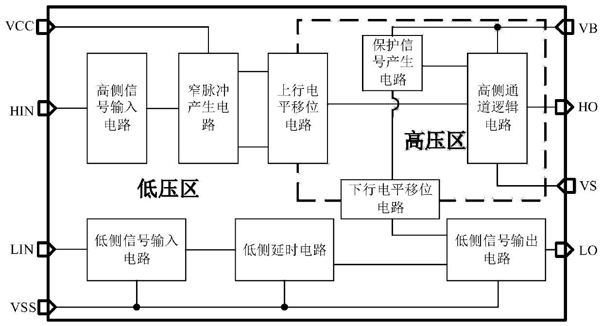
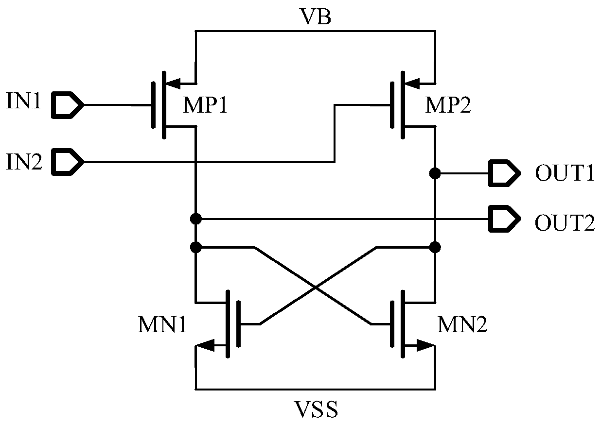
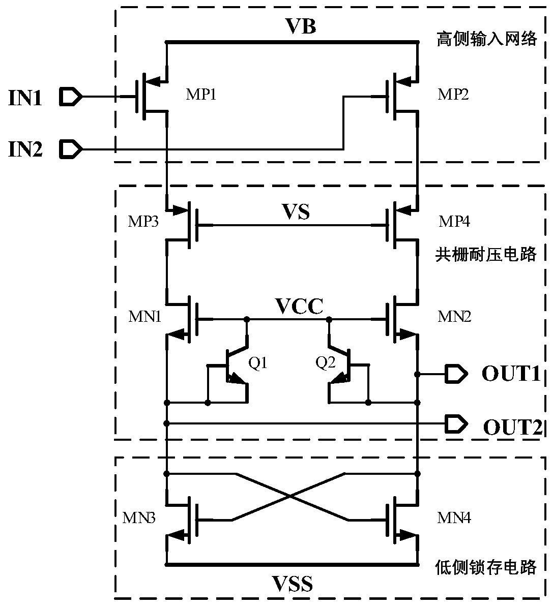
[0030] The present invention is the applicant's 2018108431121 and 2018212144290 ( Figure 4 )'s follow-up application, it can work quickly when the high-side level VB is relatively low. Its circuit architecture includes a high-side input network, a common-gate withstand voltage circuit and a low-side latch circuit, among which the high-side input network and the common-gate withstand voltage circuit are the same as Figure 4 Same, but with improvements to the low-side latch circuit.
[0031] like Figure 5 , the high-side input network (with Figure 4 In the same), the two-way PMOS common source network is composed of PMOS transistor MP1, PMOS transistor MP2 and a first-stage inverter INV. The sources of PMOS transi...
PUM
 Abstract
Description
Claims
Application Information