RC-IGBT device integrated with lateral freewheel diode by using junction terminal
A technology of freewheeling diodes and junction terminals, which is applied to semiconductor devices, electrical components, circuits, etc., can solve the problems of increasing the back plate process, easily causing negative resistance effects, and conductance modulation lag, so as to avoid premature breakdown and conductance modulation The effect is advanced and the effect of improving the voltage blocking ability
- Summary
- Abstract
- Description
- Claims
- Application Information
AI Technical Summary
Problems solved by technology
Method used
Image

Examples
Embodiment 1
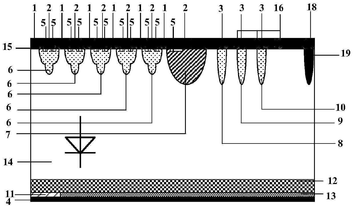
[0052] Such as Image 6 As shown, a preferred RC-IGBT device using a junction terminal integrated lateral freewheeling diode in the embodiment of the present invention includes a gate contact region 1, an emitter contact region 2, a metal field plate 3, and an N-type collector contact region 4 , P-type collector contact region 4', emitter 5, cell region P-type well 6, transition region P-type well 7, first field-limiting ring 8, second field-limiting ring 9, third field-limiting ring 10, N-type collector 11 , N-type buffer layer 12 , P-type collector 13 , N-type drift region 14 , gate oxide layer 15 and field oxide layer 16 .
[0053] The P-type collector electrode 13 completely covers the upper surface of the P-type collector electrode contact region 4'. The P-type collector 13 is doped silicon with a thickness of 1 μm, a width of 335 μm, and a doping concentration selected to the 18th power. The P-type collector contact region 4' has a width of 335 μm and a thickness of 2 ...
Embodiment 2
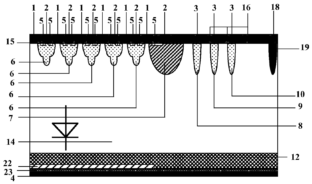
[0073] Such as Figure 7 As shown, the preferred embodiment of the present invention is an RC-IGBT device that utilizes junction terminations to integrate lateral freewheeling diodes. Three P-type buried layers 17 with the same technical parameters are added to the structure of Embodiment 1, and they are overlapped at equal intervals vertically. It is arranged at the lower ends of the first field limiting ring 8 , the second field limiting ring 9 and the third field limiting ring 10 . The P-type buried layer 17 has a width of 80 μm and a thickness of 4 μm, and the order of doping concentration is selected to the 16th power.
Embodiment 3
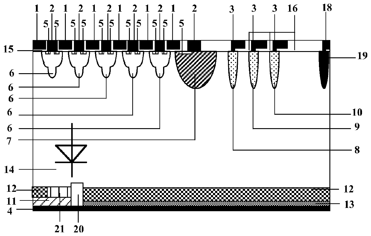
[0075] Such as Figure 8 As shown, an RC-IGBT device using a junction terminal integrated lateral freewheeling diode is preferred in the embodiment of the present invention. On the structure of Embodiment 1, an N-type collector 11 is extended to three arranged from left to right N-type collectors 11, the three N-type collectors 11 have the same technical parameters and dimensions, and the distance between them is adjustable. The middle parts of the upper surfaces of the three N-type collectors 11 are covered by the three N-type collector contact regions 4 , and the left and right sides of the upper surfaces are covered by the field oxide layer 16 .
[0076] With the help of MEDICI simulation software, it is available for the provided figure 1 As shown in the traditional RC-IGBT, as figure 2 The TPRC-IGBT that shown dielectric isolation and junction isolation combine and the novel RC-IGBT of embodiment 1 that the present invention proposes (such as Image 6 shown) for simu...
PUM
| Property | Measurement | Unit |
|---|---|---|
| Thickness | aaaaa | aaaaa |
| Thickness | aaaaa | aaaaa |
| Width | aaaaa | aaaaa |
Abstract
Description
Claims
Application Information
 - R&D Engineer
- R&D Manager
- IP Professional
- Industry Leading Data Capabilities
- Powerful AI technology
- Patent DNA Extraction
Browse by: Latest US Patents, China's latest patents, Technical Efficacy Thesaurus, Application Domain, Technology Topic.
© 2024 PatSnap. All rights reserved.Legal|Privacy policy|Modern Slavery Act Transparency Statement|Sitemap