Silicon nanocrystal/graphene wide-spectrum photodetector and preparation method thereof

A photodetector, silicon nanocrystal technology, applied in the field of photodetection, can solve the problems of affecting carrier transmission and response time as long as seconds, and achieve the effects of high responsivity, low production cost and fast response speed

Active Publication Date: 2019-12-24
NO 55 INST CHINA ELECTRONIC SCI & TECHNOLOGYGROUP CO LTD
View PDF10 Cites 3 Cited by
  • Summary
  • Abstract
  • Description
  • Claims
  • Application Information

AI Technical Summary

Problems solved by technology

The use of organic macromolecules as dispersants in colloidal quantum dots will seriously affect carrier transport, and the response time is as long as seconds

Method used


Image

  • Silicon nanocrystal/graphene wide-spectrum photodetector and preparation method thereof
  • Silicon nanocrystal/graphene wide-spectrum photodetector and preparation method thereof
  • Silicon nanocrystal/graphene wide-spectrum photodetector and preparation method thereof

Examples


preparation example Construction

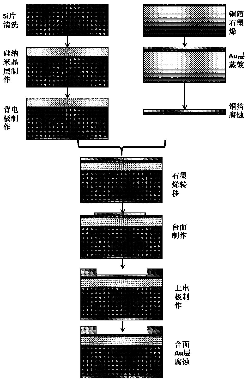
[0038] The present invention also provides a method for preparing a silicon nanocrystal / graphene wide-spectrum photodetector, comprising the following steps:

[0039] Step 1, n-type Si substrate 4 cleaning;

[0040] Step 2, preparation of silicon nanocrystalline layer 3, spin-coating HSQ photoresist at a speed of 3000 rpm, with a thickness of 0.5-0.8 μm, and annealing in a nitrogen atmosphere in a quartz annealing furnace;

[0041] Step 3. Carry out the first step of photolithography, photoetch the silicon nanocrystal mesa pattern, and use ICP etching to obtain the silicon nanocrystal mesa;

[0042] Step 4, making the back electrode layer 5, using electron beam to evaporate Ti / Au / Ti;

[0043] Step 5, making the graphene layer 2, vapor-depositing a 30-50nm Au layer on the graphene layer, and configuring a copper foil etching solution;

[0044] Step 6, transfer of the graphene layer 2, use the Si substrate sheet to transfer the graphene coated with the Au layer to clear water ...

Embodiment

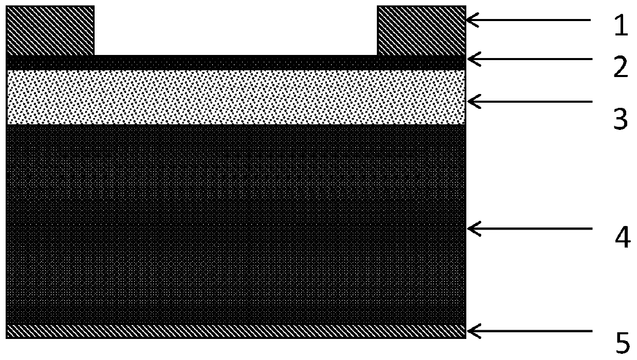
[0055] Such as figure 1 As shown, a silicon nanocrystal / graphene wide-spectrum photodetector, an n-type Si substrate 4 is followed by a silicon nanocrystal layer 3, a graphene layer 2, and a front electrode 1, and the back electrode 5 is located on the n-type Si substrate. 4 below.

[0056] n-type Si substrate 4 has a resistivity of 1-10Ω / cm and a thickness of 500 μm;

[0057] The silicon nanocrystalline layer 3 is obtained by spin-coating hydrogen silsesquioxane HSQ and annealing at a high temperature, the annealing temperature is 900-1100°C, and the thickness is 0.5-0.8 μm;

[0058]The graphene layer 2 has a single-layer structure, grown on the copper foil by CVD, and a 30nm thick gold layer is evaporated on the graphene surface, and the graphene and the gold layer are simultaneously transferred from the copper foil to the silicon nanocrystalline layer 3;

[0059] The front electrode 1 is a Ti / Au electrode, and the shape is a square electrode, such as figure 2 Shown, con...


PUM

PropertyMeasurementUnit
electrical resistivityaaaaaaaaaa
thicknessaaaaaaaaaa
thicknessaaaaaaaaaa

Abstract

The invention discloses a silicon nanocrystal/graphene wide-spectrum photodetector and a preparation method thereof. The structure comprises a back electrode, a substrate, a silicon nanocrystal layer,a graphene layer and a front electrode in order from bottom to top. The back electrode is a Ti/Au/Ti electrode. The substrate is heavily doped with n-type Si. The silicon nanocrystal layer is spin-coated with hydrogen-silsesquioxane and annealed at high temperature. The graphene layer is single-layer graphene, which is acquired by transferring vapor-deposited Au. The front electrode is a Ti/Au electrode. The photodetector provided by the invention can respond to ultraviolet, visible and near-infrared optical spectrum ranges, achieves signal doubling through the photo-switching effect betweenthe silicon nanocrystal layer and the graphene layer, has a simple preparation process, and is compatible with the CMOS process.

Description

technical field [0001] The invention relates to photoelectric detection technology, in particular to a silicon nanocrystal / graphene wide-spectrum photodetector and a preparation method thereof. Background technique [0002] Broadening the optical spectrum response range of photodetectors is the most direct and effective way to improve the ability to acquire and identify detection information. The traditional method is to simply add existing photodetectors with different band responses or to combine optoelectronic devices with certain band responses The spectral response is extended to both sides. This kind of method has limited spectral expansion effect, but causes a large increase in the volume of detection components and signal processing requirements, which is not conducive to system miniaturization and high-density integration. The wide-spectrum photodetector made of graphene material with zero bandgap can effectively expand the spectral range and reduce the volume of de...

Claims


Application Information

Patent Timeline
Patent Type & Authority Applications(China)
IPC IPC(8): H01L31/101H01L31/0216H01L31/18
CPCH01L31/02161H01L31/1013H01L31/1804Y02P70/50
Inventor 王东辰徐鹏霄王艳唐光华陈鑫龙戴丽英杨杰
Owner NO 55 INST CHINA ELECTRONIC SCI & TECHNOLOGYGROUP CO LTD
Why Eureka
Try Eureka