Manufacturing method of ultraviolet light-emitting diode epitaxial structure layer

A technology of light-emitting diodes and epitaxial structures, which is applied to electrical components, circuits, semiconductor devices, etc., can solve the problems such as the decline of the crystal quality of the epitaxial layer and the decline of the electrical conductivity, so as to simplify the design of the epitaxial structure, reduce the difficulty of preparation, and improve the overall light extraction efficiency. Effect

Active Publication Date: 2020-01-21
JIANGXI ZHAO CHI SEMICON CO LTD
View PDF6 Cites 0 Cited by
  • Summary
  • Abstract
  • Description
  • Claims
  • Application Information

AI Technical Summary

Problems solved by technology

[0006] Aiming at the deficiencies of the prior art, the present invention provides a method for preparing the epitaxial structure layer of the ultraviolet light-emitting diode, which solves the problem that the crystal quality of the epitaxial layer is sharply reduced when the Al composition is increased in the AlGaN material grown by MOCVD in the prior art. Problems with drop and rapid drop in conductivity

Method used


Image

  • Manufacturing method of ultraviolet light-emitting diode epitaxial structure layer
  • Manufacturing method of ultraviolet light-emitting diode epitaxial structure layer

Examples


Embodiment 1

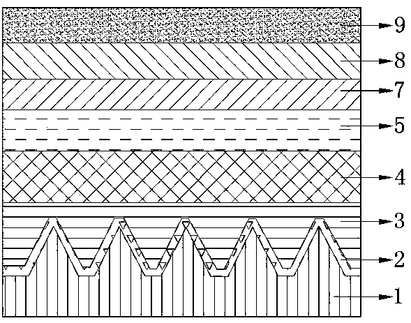
[0042] Embodiment 1, as figure 1 As shown, a method for preparing an epitaxial structure layer of an ultraviolet light-emitting diode includes a method for preparing an n-type doped AlN layer 4 by means of magnetron reactive sputtering, including the following steps:

[0043] Step S11, AlN buffer layer 2 sputtering:

[0044] S1101, the sapphire PSS sheet is introduced into the sputtering chamber, heated for 180 seconds, 120sccm nitrogen gas and 0.5sccm oxygen gas are introduced, the radio frequency power is 60W, and the radio frequency power is 90s;

[0045] S1102, 90sccm of nitrogen gas, 2sccm of oxygen gas, and 40sccm of argon gas are introduced into the sputtering chamber, the DC pulse sputtering power is set to 5000W, and the thickness of aluminum nitride with high oxygen content is deposited by sputtering to 10nm;

[0046] S1103. Inject 120 sccm of nitrogen gas into the sputtering chamber, set the RF power to 60W, and set the RF on time to 45s;

[0047] S1104, 90 sccm o...

Embodiment 2

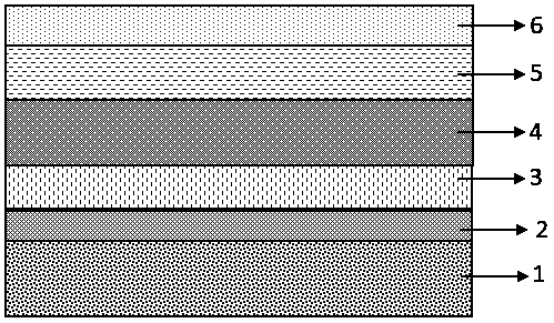
[0062] Embodiment 2, as figure 2 As shown, a method for preparing an epitaxial structure layer of an ultraviolet light-emitting diode includes a preparation method for realizing an n-type doped AlN layer 4 by magnetron reactive sputtering and a method for realizing a p-type doped AlN layer 6 by magnetron reactive sputtering. The preparation method comprises the following steps:

[0063] Step S1, AlN buffer layer 2 sputtering:

[0064] S1101, the sapphire flat sheet is introduced into the sputtering chamber, heated for 180 seconds, 120sccm nitrogen gas and 0.5sccm oxygen gas are introduced, the radio frequency power is 60W, and the radio frequency power is 90s;

[0065] S1102, 90sccm of nitrogen gas, 2sccm of oxygen gas, and 40sccm of argon gas are introduced into the sputtering chamber, the DC pulse sputtering power is set to 5000W, and the thickness of aluminum nitride with high oxygen content is deposited by sputtering to 10nm;

[0066] S1103. Inject 120 sccm of nitrogen ...


PUM

PropertyMeasurementUnit
thicknessaaaaaaaaaa
thicknessaaaaaaaaaa
thicknessaaaaaaaaaa

Abstract

The invention discloses a manufacturing method of an ultraviolet light-emitting diode epitaxial structure layer. The method comprises an AlN buffer layer, a non-doped AlN thin film layer, an n-type doped AlN layer, an active layer and a p-type doped AlN layer, wherein the AlN buffer layer, the non-doped AlN thin film layer and the n-type doped AlN layer successively grow on a sapphire substrate through a sputter coating mode, the active layer grows through an MOCVD mode, and the p-type doped AlN layer grows through the sputter coating mode. The method has advantages that the MOCVD grows through a physical sputtering mode, a high-quality AlN material which is not easy to grow is grown, and n-type Si doping and p-type Mg doping are realized; based on that, growth of an AlGaN active layer with s higher Al content by the MOCVD is easier to realize; an ultraviolet light emitting diode can emit ultraviolet light with a shorter wavelength; therefore, an epitaxial structure design of the ultraviolet light-emitting diode is simplified, manufacturing difficulty of the ultraviolet light-emitting diode is reduced, and overall light-emitting efficiency of the ultraviolet light-emitting diode isimproved because a p-type doped GaN ohmic contact epitaxial layer capable of absorbing the ultraviolet light does not need to be manufactured.

Description

technical field [0001] The invention relates to the technical field of light-emitting diode preparation, in particular to a method for preparing an epitaxial structure layer of an ultraviolet light-emitting diode. Background technique [0002] UltraViolet Light Emitting Diode (UV LED for short) has attracted much attention because of its huge potential application value in the fields of sterilization and disinfection, environmental purification and short-distance safe communication. At present, ultraviolet LEDs are mainly based on aluminum gallium nitride (AlGaN) materials, in which the aluminum (Al) component is improved to obtain shorter wavelength deep ultraviolet LEDs. However, the current AlGaN material grown based on MOCVD (Metal Organic Chemical Vapor Deposition, metal organic compound chemical vapor deposition) will lead to a sharp decline in the crystal quality of the epitaxial layer when the Al composition is increased, and the increase in the Al composition will a...

Claims


Application Information

Patent Timeline
Patent Type & Authority Applications(China)
IPC IPC(8): H01L33/00
CPCH01L33/007
Inventor 武良文
Owner JIANGXI ZHAO CHI SEMICON CO LTD
Why Eureka
Try Eureka