Defect operating system and device of semiconductor factory

An operating system and semiconductor technology, applied in semiconductor/solid-state device manufacturing, general control systems, control/regulation systems, etc., can solve problems such as poor performance, limited scanning electron microscope photography speed, and difficulty in finding failures

Active Publication Date: 2020-01-24
ELITETECH TECH
View PDF12 Cites 5 Cited by
  • Summary
  • Abstract
  • Description
  • Claims
  • Application Information

AI Technical Summary

Problems solved by technology

Obviously, through this sampling process, it is very difficult to find system defects that actually cause open or short-circuit failures
In addition, if the real system defect is not among the 500 system defect graphic groups, the semiconductor factory will not be able to accurately and real-time provide the SEM photos of the system defects that cause the failure rate to the process engineer, and it will be difficult to use the SEM photos of the system defects To analyze the source of system defects in the process, optical approximation correction, and layout diagrams, delay the time to improve the yield of system defects, and increase the cost of semiconductor factories and IC design companies
[0005] In terms of random defect detection, as the size of the semiconductor manufacturing process shrinks, the number of random defects also increases greatly due to the reduction in size. Therefore, each random def

Method used


Image

  • Defect operating system and device of semiconductor factory
  • Defect operating system and device of semiconductor factory
  • Defect operating system and device of semiconductor factory

Examples


Embodiment Construction

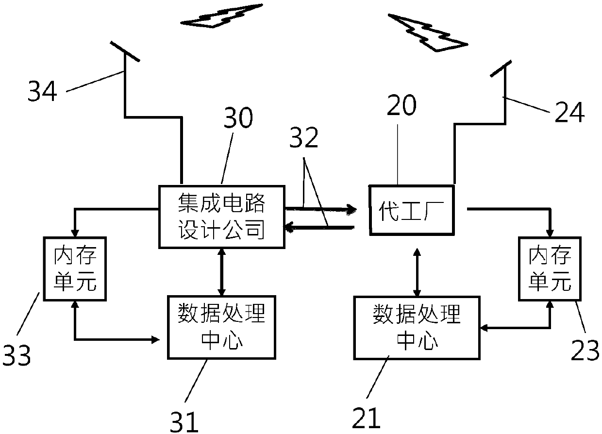
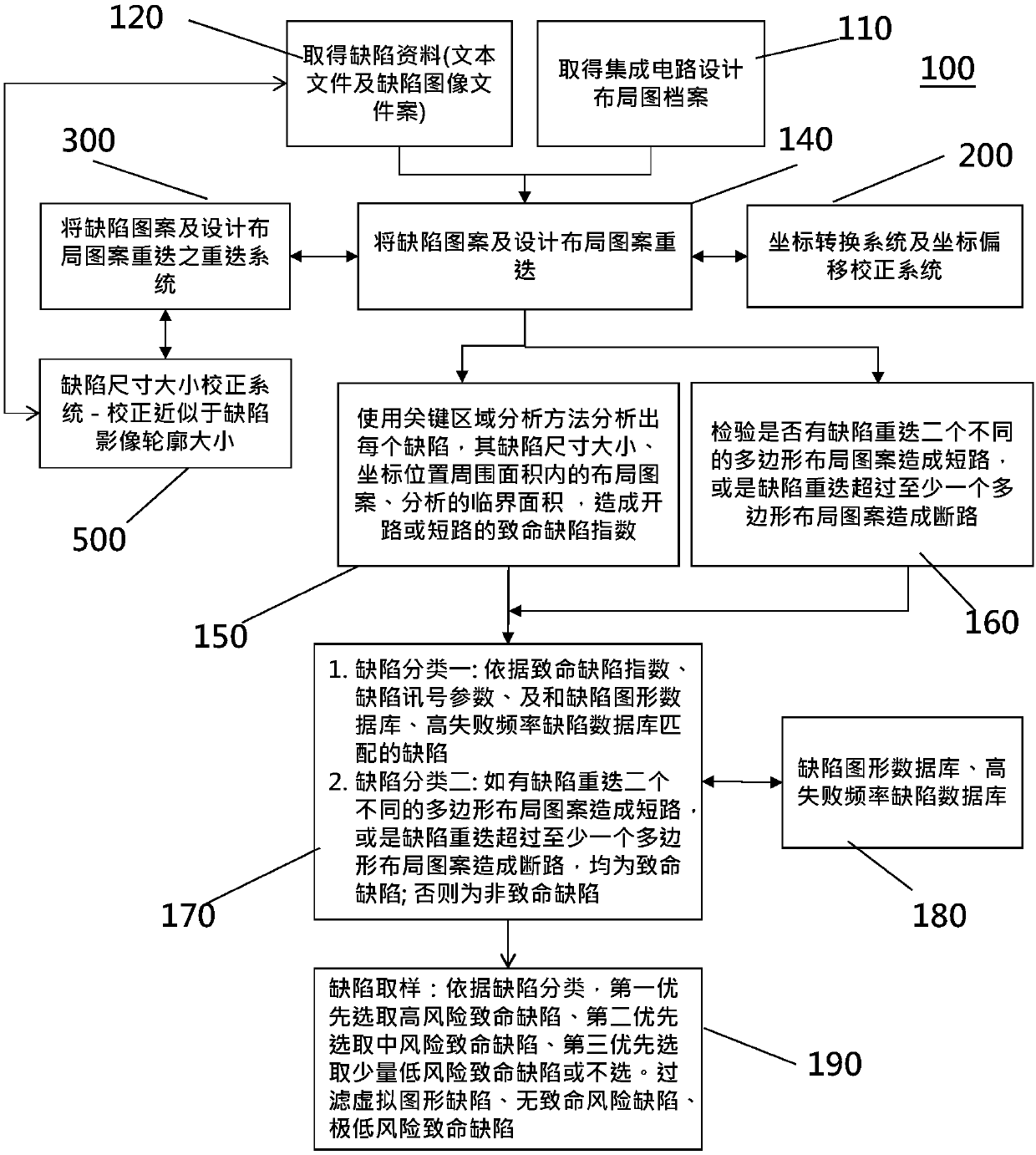
[0081] In semiconductor manufacturing plants, semiconductor packaging manufacturing plants, flat panel display manufacturing plants, solar panel manufacturing plants, printed circuit board manufacturing plants, photomask manufacturing plants, LED manufacturing or assembly plants, it is necessary to pass through photomasks, semiconductor lithography, Etching and thin film deposition and other equipment and process methods to form products with specific functions; due to many complicated steps in the manufacturing process, control of process and equipment parameters, deviation of equipment parameters, material and gas purity, or technical bottlenecks all cause Defects that affect product yield are unavoidable. Therefore, during the manufacturing process of semiconductor factories, defect detection and analysis are performed to improve yield and reduce costs.

[0082] In addition, the "semiconductor factory defect operating system" described in the present invention includes: app...


PUM


Abstract

The invention discloses a defect operating system of a semiconductor factory. The defect operating system of the semiconductor factory is used for immediately processing a plurality of defect data; then, coordinate correction, defect size correction and analysis by using critical area analysis are carried out to generate a fatal defect data file; then, an integrated circuit design company carriesout fault analysis and generates failure fatal defect data to generate new design layout data; and finally, the new design layout data and the failure fatal defect data are transmitted back to the semiconductor factory through a network. The defect operating system of the semiconductor factory is used for mutually paying and feeding back defect data and solving the root cause of the defect by theintegrated circuit design company and the semiconductor factory so as to achieve the purpose of improving the yield.

Description

technical field [0001] The present invention relates to a defect operating system and a device in the process of manufacturing wafers into functional chips by a semiconductor factory; in particular, it relates to a device used in IC design companies and semiconductor manufacturing factories, IC design companies and semiconductor packaging manufacturing factories , IC design company and printed circuit board manufacturing factory, IC design company and photomask manufacturing factory, design company and flat panel display manufacturing factory, design company and solar panel manufacturing factory, design company and LED manufacturing or semiconductor factory defect operation of assembly factory systems and devices. Background technique [0002] Generally speaking, after the integrated circuit design company or IC design company completes the functional circuit design, it needs to entrust the semiconductor fab to manufacture according to the IC design layout designed by it. O...

Claims


Application Information

Patent Timeline
IPC IPC(8): G05B19/418H01L21/67
CPCG05B19/4183H01L21/67242Y02P90/02
Inventor 吕一云蔡瑞圳
Owner ELITETECH TECH
Why Eureka
Try Eureka