
Plasma terahertz waveguide generating device

A plasma and generation device technology, applied in the field of plasma, can solve the problems of inability to perform continuous adjustment, unable to reconfigure the structure, slow response speed, etc. Effect

Active Publication Date: 2020-02-18
NANJING UNIV OF AERONAUTICS & ASTRONAUTICS
View PDF15 Cites 1 Cited by
  • Summary
  • Abstract
  • Description
  • Claims
  • Application Information

AI Technical Summary

Problems solved by technology

The disadvantage of this patent application is that the medium used is alumina ceramics and nickel-zinc ferrite, and its dielectric constant and other parameters are fixed. It can only work in the X-band with a wavelength of 3cm, and the structure cannot be reconstructed. Only one form of waveguide that can realize T shape
The disadvantage of this patent is that the metal pillar needs to be inserted or pulled out of the photonic crystal structure through a mechanical device, the response speed is slow, continuous adjustment cannot be performed, the operation is complicated, and only linear waveguides can be realized.
The plasma discharge tube of this patent has a wall thickness of 1mm, an outer diameter of 12mm, and a length of 250mm, and is filled with argon gas with a pressure of 650Pa and a purity of 99.99%. When the discharge voltage is between 20-30kV, the plasma density changes Range is 10 11 cm -3 -9×10 11 cm -3 The disadvantage of this patent is that there is only one plasma defect, the working mode and range are fixed, and it can only realize the filtering function with a resonant frequency of 7.7GHZ-8.5GHz and a forbidden band width of 7.2GHz-10.5GHz

Method used

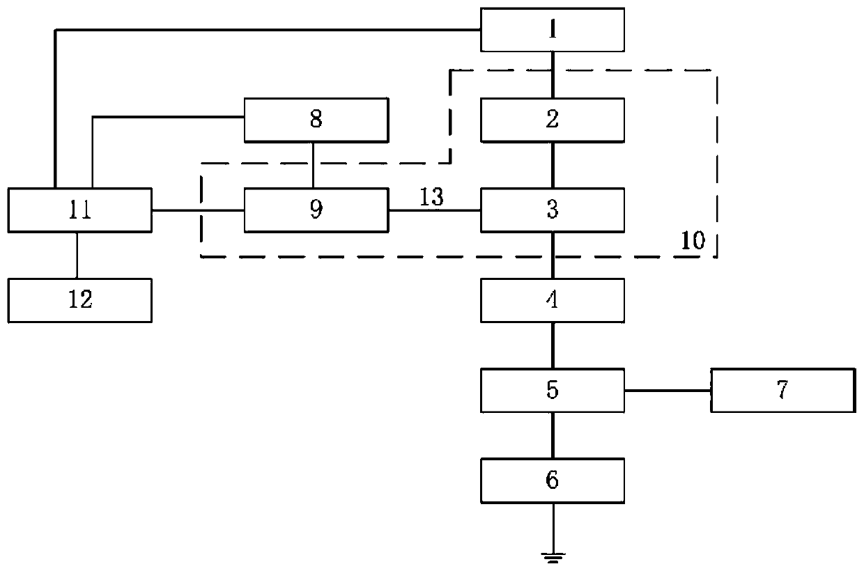
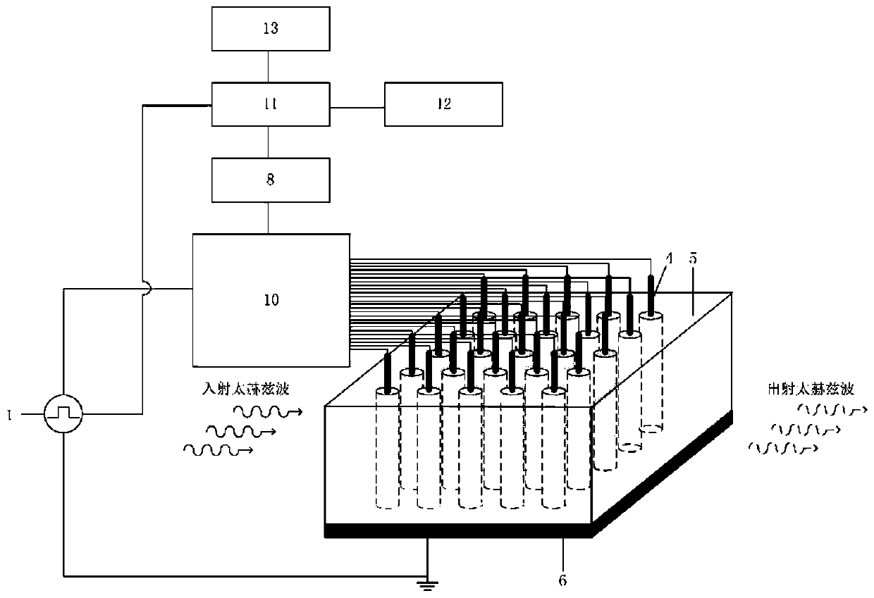

Image

  • Plasma terahertz waveguide generating device
  • Plasma terahertz waveguide generating device
  • Plasma terahertz waveguide generating device

Examples


Embodiment 1

[0047] In this embodiment, the parameters of the high-voltage pulse power supply are voltage 0-20kV, frequency 1-30kHz, output pulse width 5μs, pulse rising edge less than 1μs. The number of resistors, high-voltage solid-state switches, drive modules, needle electrodes, and micro-vias is 25. The parameter of the resistance is 1kΩ / 1000W; the withstand voltage value of the high-voltage solid-state switch is 20kV, the maximum allowable effective current value is 20A, and the turn-on and turn-off time is 1μs; the material of the needle electrode is copper, and the needle body is inserted into the through hole of the dielectric board The inner part has an insulating coating on the outside. The insulating layer is made of epoxy resin with a thickness of 60 μm; the size of the dielectric board is 6 mm long x 6 mm wide x 5 mm thick, and there are 5 x 5 through holes in the center with a diameter of 300 μm. The pitch is 500 μm; the size of the ground electrode is 5 mm long×5 mm wide×1 ...

Embodiment 2

[0050] In this implementation, the parameters of the high-voltage pulse power supply are voltage 0-20kV, frequency 1-50kHz, output pulse width 1-50μs, and pulse rising edge less than 1μs. The number of resistors, high-voltage solid-state switches, drive modules, needle electrodes, and micro-vias is 70. The parameter of the resistor is 5kΩ / 500W; the withstand voltage of the high-voltage solid-state switch is 20kV, the maximum allowable effective current is 20A, and the turn-on and turn-off time is 1μs; the material of the needle electrode is copper, and the needle body is inserted into the through hole of the dielectric board The inner part has an insulating coating on the outside, and the insulating layer is made of epoxy resin with a thickness of 30 μm; the size of the dielectric board is 5 mm long x 6 mm wide x 5 mm thick, and there are 7 x 10 through holes in the center with a diameter of 100 μm. The pitch is 200 μm; the size of the ground electrode is 5mm long×5mm wide×1mm...


PUM

PropertyMeasurementUnit
thicknessaaaaaaaaaa
thicknessaaaaaaaaaa
thicknessaaaaaaaaaa

Abstract

The invention discloses a plasma terahertz waveguide generation device, which comprises a microcontroller, a man-machine interaction module, a power supply, a high-voltage pulse power supply, a groundelectrode, a dielectric plate and high-voltage pulse branches, wherein a micro through hole array penetrating through the whole dielectric plate is arranged on the dielectric plate; one high-voltagepulse branch corresponds to one micro through hole; each high-voltage pulse branch comprises a resistor, a high-voltage solid-state switch, a driving module and a pin electrode; each pin electrode isinserted into the corresponding micro through hole from the upper surface of the dielectric plate; the outer surface of each pin electrode is tightly attached to the inner surface of the correspondingmicro through hole; the ground electrode is tightly attached to the lower surface of the dielectric plate; the two ends of the micro through hole array are sealed through the pin electrodes and the ground electrode; and each micro through hole contains working gas. Electric control type adjustment of photonic crystal band gap characteristics can be realized, and the device has the characteristicsof fast dynamic response, reconfigurability and wide adjustment frequency band.

Description

technical field [0001] The invention belongs to the field of terahertz technology and discharge plasma technology, and in particular relates to plasma terahertz waveguide technology. Background technique [0002] Terahertz (THz) wave refers to the frequency of 0.1 ~ 10THz (wavelength 30 ~ 3000μm, 1THz = 10 12 Hz) range of electromagnetic waves. THz technology is widely used in many important fields such as biomolecular identification, material diagnosis, astronomical observation, atmospheric and environmental monitoring, wireless communication, national security and anti-terrorism. In the THz application system, the transmission channel of terahertz waves—the waveguide is an indispensable key part. [0003] Photonic crystals are artificial microstructures with periodic arrangements, which have the characteristics of photonic band gap and photonic localization, and can be used to make terahertz waveguides. In the photonic forbidden band of photonic crystals, electromagneti...

Claims


Application Information

Patent Timeline
Patent Type & Authority Applications(China)
IPC IPC(8): H05H1/48H01P11/00H01P3/16G02B6/13G02B6/122
CPCG02B6/1225G02B6/13H01P3/16H01P11/006H05H1/48H05H1/471
Inventor 吴淑群杨璐陈玉秀顾亚楠张潮海
Owner NANJING UNIV OF AERONAUTICS & ASTRONAUTICS
Learn More