Semiconductor device based on composite substrate and preparation method thereof

A composite substrate and semiconductor technology, applied in the field of microelectronics, can solve problems affecting the quality of semiconductor devices, low thermal conductivity of Si substrates, slow heat dissipation of semiconductor devices, etc., to avoid device failure, improve heat dissipation efficiency, and increase yield Effect

Inactive Publication Date: 2020-02-21
XIDIAN UNIV
View PDF15 Cites 4 Cited by
  • Summary
  • Abstract
  • Description
  • Claims
  • Application Information

AI Technical Summary

Problems solved by technology

[0004] However, the thermal conductivity of the Si substrate is low, and the direct growth of nitride materials on the Si substrate will cause problems such as slow heat dissipation of the semiconductor device and defects in the crystal lattice, which will affect the quality of the semiconductor device.

Method used


Image

  • Semiconductor device based on composite substrate and preparation method thereof
  • Semiconductor device based on composite substrate and preparation method thereof
  • Semiconductor device based on composite substrate and preparation method thereof

Examples


Embodiment 1

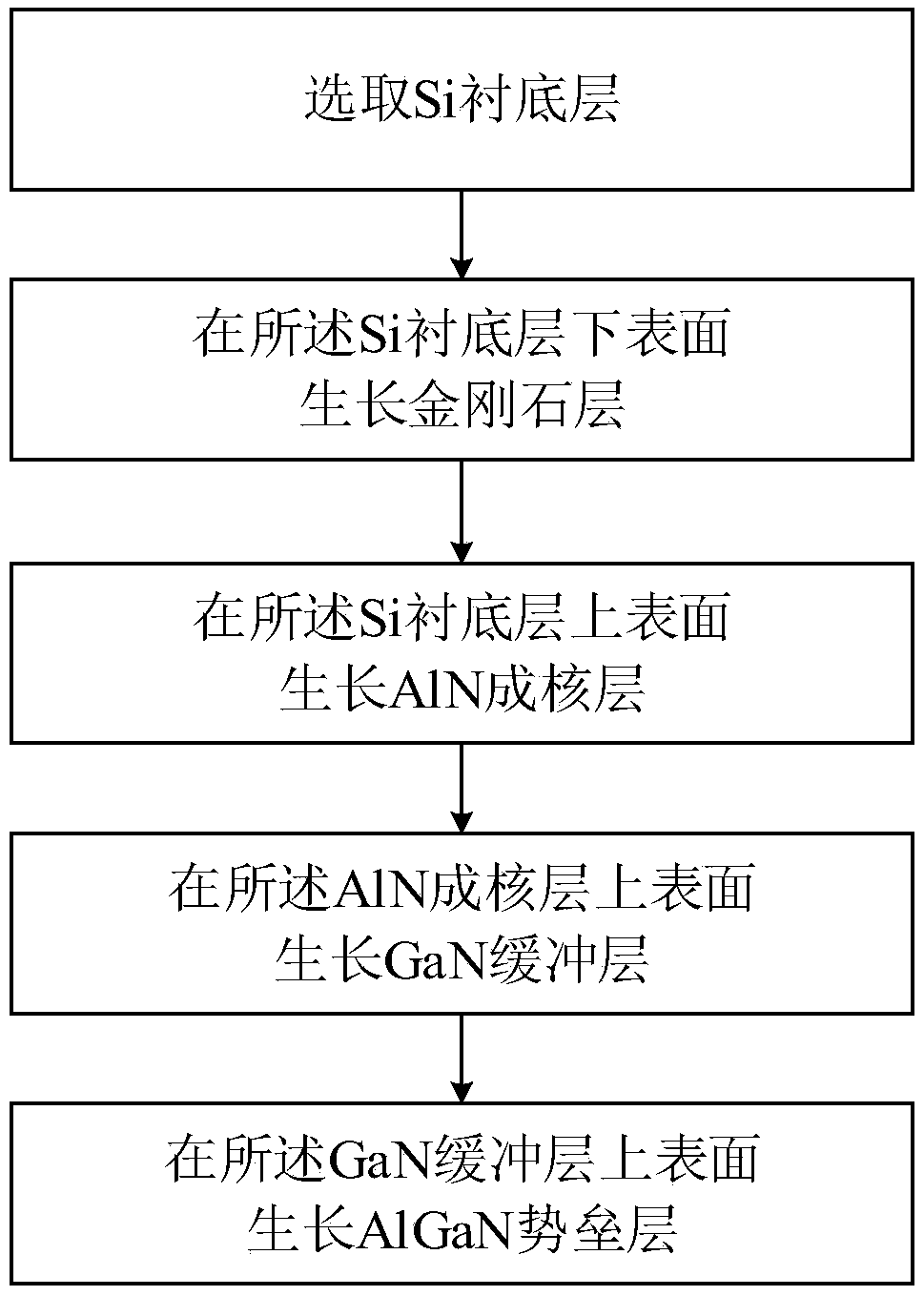
[0036] See figure 1 , figure 1 It is a schematic flowchart of a method for manufacturing a semiconductor device based on a composite substrate provided by an embodiment of the present invention. An embodiment of the present invention provides a method for preparing a semiconductor device based on a composite substrate, the method comprising the following steps:

[0037] Step 1. Select the Si substrate layer.

[0038] Step 2, growing a diamond layer on the lower surface of the Si substrate layer.

[0039] See Figure 2a , Figure 2a A flow chart of a manufacturing process of a semiconductor device based on a composite substrate provided by an embodiment of the present invention. Specifically, a diamond layer with a thickness of 30-200 μm is grown on the lower surface of the Si substrate layer by using Microwave Plasma Chemical Vapor Deposition (MPCVD for short). The process conditions are as follows: the gas used in the reaction chamber of the microwave plasma chemical va...

Embodiment 2

[0057] see again Figure 2a-2d , the present invention introduces the specific preparation methods of the embodiments of the present invention on the basis of the above-mentioned embodiments. The preparation method of the embodiment of the present invention comprises the following steps:

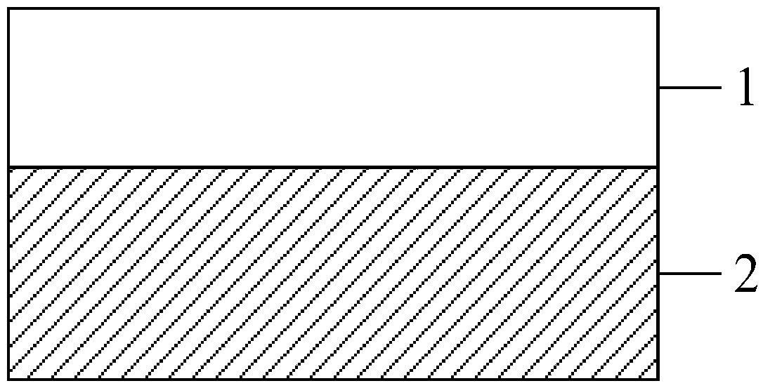
[0058] S1. Select the Si substrate layer 1 .

[0059] Preferably, the Si substrate layer 1 with a thickness of 1.5 mm is selected as the initial material.

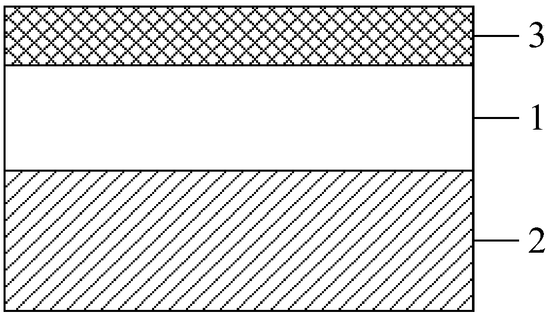
[0060] S2 , growing a diamond layer 2 on the lower surface of the Si substrate layer 1 .

[0061] see again Figure 2a , using a chemical vapor deposition method to grow a diamond layer 2 on the lower surface of the Si substrate layer 1;

[0062] Specifically, a diamond layer 2 with a thickness of 30 μm was grown on the lower surface of the Si substrate layer 1 by MPCVD. The process conditions are as follows: the gas in the MPCVD reaction chamber is a mixed gas of methane and hydrogen, the total flow rate of the mixed gas is 200 scc...

Embodiment 3

[0081] see again Figure 2a-2d , the present invention introduces the specific preparation methods of the embodiments of the present invention on the basis of the above-mentioned embodiments. The preparation method of the embodiment of the present invention comprises the following steps:

[0082] S1. Select the Si substrate layer 1 .

[0083] Preferably, the Si substrate layer 1 with a thickness of 1.5 mm is selected as the initial material.

[0084] S2 , growing a diamond layer 2 on the lower surface of the Si substrate layer 1 .

[0085] See you again Figure 2a , using a chemical vapor deposition method to grow a diamond layer 2 on the lower surface of the Si substrate layer 1;

[0086] Specifically, a diamond layer 2 with a thickness of 200 μm was grown on the lower surface of the Si substrate layer 1 by MPCVD. The process conditions are as follows: the gas in the MPCVD reaction chamber is a mixed gas of methane and hydrogen, the total flow rate of the mixed gas is 10...


PUM

PropertyMeasurementUnit
thicknessaaaaaaaaaa
thicknessaaaaaaaaaa
thicknessaaaaaaaaaa

Abstract

The invention relates to a semiconductor device based on a composite substrate and a preparation method thereof. The preparation method comprises steps of selecting a Si substrate layer; growing a diamond layer on a lower surface of the Si substrate layer; growing an AlN nucleating layer on an upper surface of the Si substrate layer; growing a GaN buffer layer on an upper surface of the AlN nucleating layer; and growing an AlGaN barrier layer on an upper surface of the GaN buffer layer. The preparation method is advantaged in that the Si substrate layer with high quality and the diamond layerwith high thermal conductivity are combined to form the Si/diamond composite substrate structure, and high thermal conductivity of the diamond layer is utilized to solve a problem of poor heat dissipation caused by growing a high-power nitride semiconductor material purely on the Si substrate layer.

Description

technical field [0001] The invention belongs to the technical field of microelectronics, and in particular relates to a semiconductor device based on a composite substrate and a preparation method thereof. Background technique [0002] Semiconductor devices are the basis of power electronics technology and its application devices. Semiconductor devices are used in almost all electronic manufacturing industries, including notebooks, servers, monitors in the computer field, and electronic equipment such as mobile phones and telephones. Semiconductor devices made of nitrides have great application potential in high-frequency, high-voltage, and high-power semiconductor devices due to their advantages such as large band gap, high carrier mobility, and strong breakdown field. [0003] Because it is extremely difficult to grow nitride large-scale semiconductors, all mature devices are now based on substrates such as Si. Since the Si substrate has the advantages of low cost, large ...

Claims


Application Information

Patent Timeline
Patent Type & Authority Applications(China)
IPC IPC(8): H01L21/02H01L23/373
CPCH01L21/02381H01L21/0254H01L23/3732
Inventor 任泽阳张雅超张进成张金风许晟瑞苏凯郝跃
Owner XIDIAN UNIV
Why Eureka
Try Eureka