

Semiconductor device based on SiC/diamond composite substrate layer and preparation method thereof
A diamond layer and substrate layer technology, applied in the field of microelectronics, can solve the problems of affecting the heat dissipation capability of semiconductor devices, limiting the application of semiconductor devices, poor thermal conductivity of epitaxial substrates, etc., so as to reduce manufacturing complexity and cost, and avoid device failure. , The effect of improving heat dissipation efficiency
- Summary
- Abstract
- Description
- Claims
- Application Information
AI Technical Summary
Problems solved by technology
Method used
Image

Examples
Embodiment 1
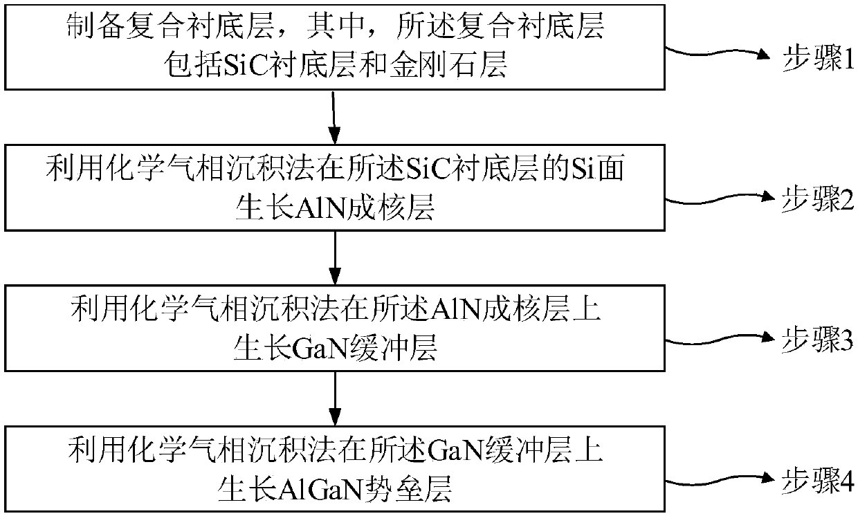
[0037] See figure 1 , figure 1 It is a schematic flowchart of a method for preparing a semiconductor device based on a SiC / diamond composite substrate layer provided by an embodiment of the present invention. The preparation method comprises the following steps:
[0038] Step 1, preparing a composite substrate layer, wherein the composite substrate layer includes a SiC substrate layer and a diamond layer;
[0039] Step 1.1, selecting the SiC substrate layer;
[0040] Step 1.2, growing a diamond layer on the C-face of the SiC substrate layer;
[0041] See Figure 2a , Figure 2a A flow chart of a manufacturing process of a semiconductor device based on a SiC / diamond composite substrate layer provided by an embodiment of the present invention. Specifically, the selected SiC substrate layer is put into a Microwave Plasma Chemical Vapor Deposition (MPCVD) reaction chamber, a mixed gas of hydrogen and methane is introduced into the reaction chamber, and the SiC substrate laye...
Embodiment 2
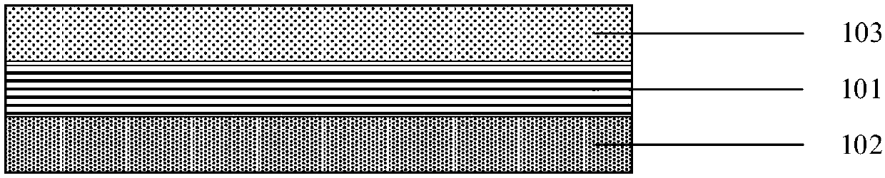
[0071] See Figure 2a-2d , Figure 2a-2d A flow chart of a manufacturing process of a semiconductor device based on a SiC / diamond composite substrate layer provided by an embodiment of the present invention. This preparation method comprises the steps:
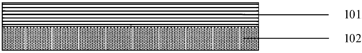
[0072] Step 1, preparing a composite substrate layer, wherein the composite substrate layer includes a SiC substrate layer 101 and a diamond layer 102;
[0073] Step 1.1, selecting the SiC substrate layer 101;
[0074] Preferably, the SiC substrate layer 101 with a thickness of 0.3-1 mm is selected as the initial material.
[0075] Step 1.2, growing a diamond layer 102 on the C-face of the SiC substrate layer 101;
[0076] see you again Figure 2a , grow a diamond layer 102 on the C-plane of the SiC substrate layer 101 . Specifically, the selected SiC substrate layer 101 is put into the MPCVD reaction chamber, and a mixed gas of hydrogen and methane is introduced into the MPCVD reaction chamber;
[0077] The process con...
Embodiment 3
[0106] See Figure 2a-2d , Figure 2a-2d A flow chart of a manufacturing process of a semiconductor device based on a SiC / diamond composite substrate layer provided by an embodiment of the present invention. This preparation method comprises the steps:
[0107] Step 1, preparing a composite substrate layer, wherein the composite substrate layer includes a SiC substrate layer 101 and a diamond layer 102;
[0108] Step 1.1, selecting the SiC substrate layer 101;
[0109] Preferably, the SiC substrate layer 101 with a thickness of 0.3-1 mm is selected as the initial material.
[0110] Step 1.2, growing a diamond layer 102 on the C-face of the SiC substrate layer 101;
[0111] see you again Figure 2a , grow a diamond layer 102 on the C-plane of the SiC substrate layer 101 . Specifically, the selected SiC substrate layer 101 is put into the MPCVD reaction chamber, and a mixed gas of hydrogen and methane is introduced into the MPCVD reaction chamber;
[0112] The process con...
PUM
| Property | Measurement | Unit |
|---|---|---|
| Thickness | aaaaa | aaaaa |
| Thickness | aaaaa | aaaaa |
| Thickness | aaaaa | aaaaa |
Abstract
Description
Claims
Application Information